|
|
|
PDF XZ1002-BD Data sheet ( Hoja de datos )
| Número de pieza | XZ1002-BD | |
| Descripción | highly integrated dual path transmit/receive 3 port core chip | |
| Fabricantes | M/a-com | |
| Logotipo | ||
Hay una vista previa y un enlace de descarga de XZ1002-BD (archivo pdf) en la parte inferior de esta página. Total 11 Páginas | ||
|
No Preview Available !
DataSheet.in
XZ1002-BD
8.5-11.0 GHz GaAs MMIC
Core Chip
Rev 01-Sep-10
Features
• Highly Integrated Core Chip
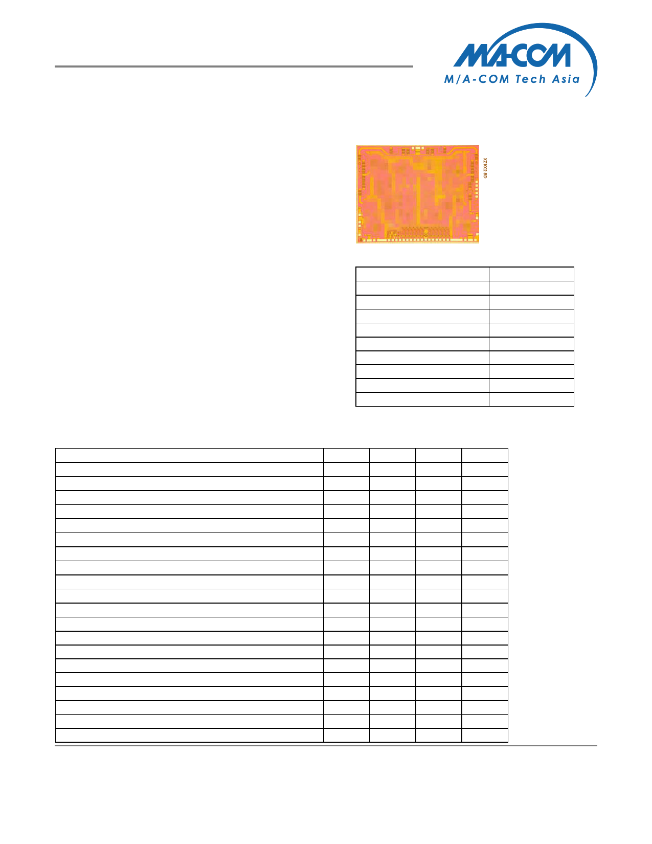
Chip Device Layout
• Transmit and Receive Modes of Operation
• Integrated T/R Switches, LNA and Driver Amplifier,
6-Bit Phase Shifter and 5-Bit Attenuator
• 21.0 dB Small Signal RX Gain
• +23.5 dBm TX P1dB Compression Point
• Compensated On-Chip Gate Bias Circuit
• Parallel Data Input
• 100% On-Wafer RF, DC and Output Power Testing
Absolute Maximum Ratings
• 100% Visual Inspection to MIL-STD-883 Method 2010 Supply Voltage (Vd)
6V
General Description
The XZ1002-BD is a highly integrated dual path transmit/receive 3
port core chip. It is designed for applications operating within the
8.5 to 11.0 GHz range. The core consists of integrated
transmit/receive switches, LNA, 6-bit phase shifter, 5-bit attenuator
and driver amplifier. The digital control logic allows for parallel
data input so that the phase shifter and attenuator may be
changed instantaneously. The chip has surface passivation to
protect and provide a rugged part with backside via holes and gold
metallization to allow either a conductive epoxy or eutectic solder
die attach process. This device is well suited for phased array
radar applications.
Gate Supply (Vs)
-6V to -4V
Logic Supply (Vl)
0 to 5.5V
Supply Current (Id)
350 mA
Input Power
TBD
Input Power RX
+20 dBm
Input Power RFCOM
+15 dBm
Storage Temperature (Tstg) -65 to +165 ºC
Operating Temperature (Ta) -55 to MTTF Graph1
Channel Temperature
MTTF Graph1
(1) Channel temperature affects a device's MTTF. It is recommended
to keep channel temperature as low as possible for maximum life.
Electrical Characteristics (Ambient Temperature T=25 oC)
Parameter
Frequency Range (f)
Input Return Loss RX/TX Mode (S11)
Output Return Loss RX/TX Mode (S22)
Receive Small Signal Gain (S21)
Transmit Small Signal Gain (S21)
Receive Output Power for 1 dB Compression Point (P1dB)
Transmit Output Power for 1 dB Compression Point (P1dB)
Receive Noise Figure (NF)
Receive Output Third Order Intercept (OIP3)
Phase Shifter Range (6 Bit, 64 states, 5.625 deg step)
RMS Phase Error
Attenuator Range (5 Bit, 32 states, 0.9 dB step)
RMS Attenuator Amplitude Error
Drain Bias Voltage (Vd1,2,3,4)
Gate Bias Voltage (Vs1,2,3)
Control Voltage High (Va0,1,2,3,4) & (Vp0,1,2,3,4,5)
Control Voltage Low (Va0,1,2,3,4) & (Vp0,1,2,3,4,5)
Supply Current (Id) (Vd=4V, TX mode)
Supply Current (Ia) (Vs=-5V)
Supply Current (Il) (Vl=3.3V)
Units
GHz
dB
dB
dB
dB
dBm
dBm
dB
dBm
deg
deg
dB
dB
VDC
VDC
VDC
VDC
mA
mA
mA
Min.
8.5
0
0
-
-4.0
+2.0
0.0
Typ.
15.0
15.0
21.0
19.0
17.5
23.5
5.2
+28.0
1.5
0.3
+4.0
-5.0
+3.3
-
280
35
9.5
Max.
11
355
28.5
+4.5
+5.0
+0.8
Page 1 of 11
ADVANCED: Data sheets contain information regarding a product M/A-COM Tech Asia is
considering for development. Performance is based on target specifications, simulated results,
and/or prototype measurements. Commitment to develop is not guaranteed.
PRELIMINARY: Data sheets contain information regarding a product M/A-COM Tech Asia has
under development. Performance is based on engineering tests. Specifications are typical.
Mechanical outline has been fixed. Engineering samples and/or test data may be available.
Commitment to produce in volume is not guaranteed.
3F, 3-2 Industry East IX Road, Science-Based Industrial Park
Hsinchu 30075 Taiwan, R.O.C
Tel +886-3-567-9680 / Fax +886-3-567-9433
Email [email protected]
Visit macomtechasia.com for additional data sheets and product information.
Characteristic data and specifications are subject to change without notice.
©2010 M/A-COM Tech Asia
1 page 
DataSheet.in
XZ1002-BD
8.5-11.0 GHz GaAs MMIC
Core Chip
Rev 01-Sep-10
Measurements (cont.)
Large Signal Performance
Sample measured at Ta=35 C
26
24
22
20 8.5 GHz
18 8.75 GHz
9 GHz
16 9.25 GHz
14 9.5 GHz
12 9.75 GHz
10
-15 -14 -13 -12 -11 -10 -9 -8 -7 -6 -5 -4 -3 -2 -1 0 1
Pin (dBm)
10 GHz
10.25 GHz
10.5 GHz
10.75 GHz
11 GHz
23 45
Large Signal Performance
Sample measured at Ta=35 C
22
20
18
16 8.5 GHz
14 8.75 GHz
12 9 GHz
10 9.25 GHz
8 9.5 GHz
6 9.75 GHz
4
-15 -14 -13 -12 -11 -10 -9 -8 -7 -6 -5 -4 -3 -2 -1 0 1
Pin (dBm)
10 GHz
10.25 GHz
10.5 GHz
10.75 GHz
11 GHz
2 345
15
14
13
12
11
10
9
8
7
6
5
7
IIP3 versus Temperature in Receive Mode
Ta=10_C
Ta=35_C
Ta=60_C
7.5 8 8.5 9 9.5 10 10.5 11 11.5 12
Frequency [GHz]
35
34
33
32
31
30
29
28
27
26
25
7
OIP3 versus Temperature in Receive Mode
T a=1 0 _ C
T a=3 5 _ C
T a=6 0 _ C
7.5 8 8.5 9 9.5 10 10.5 11 11.5 12
Frequency [GHz]
Gain Phase Plots
Measured in RX-mode at f=10 GHz and Ta=35 °C
360
315
270
225
180
135
90
45
0
0 2 4 6 8 10 12 14 16 18 20 22 24 26 28 30
Attenuation [dB]
Measured in TX-mode at f=10 GHz and Ta=35 °C
360
315
270
225
180
135
90
45
0
0 2 4 6 8 10 12 14 16 18 20 22 24 26 28 30
Attenuation [dB]
ADVANCED: Data sheets contain information regarding a product M/A-COM Tech Asia is
considering for development. Performance is based on target specifications, simulated results,
and/or prototype measurements. Commitment to develop is not guaranteed.
PRELIMINARY: Data sheets contain information regarding a product M/A-COM Tech Asia has
under development. Performance is based on engineering tests. Specifications are typical.
Mechanical outline has been fixed. Engineering samples and/or test data may be available.
Commitment to produce in volume is not guaranteed.
Page 5 of 11
3F, 3-2 Industry East IX Road, Science-Based Industrial Park
Hsinchu 30075 Taiwan, R.O.C
Tel +886-3-567-9680 / Fax +886-3-567-9433
Email [email protected]
Visit macomtechasia.com for additional data sheets and product information.
Characteristic data and specifications are subject to change without notice.
©2010 M/A-COM Tech Asia
5 Page 
DataSheet.in
XZ1002-BD
8.5-11.0 GHz GaAs MMIC
Core Chip
Rev 01-Sep-10
Handling and Assembly Information
CAUTION! - M/A-COM Tech Asia MMIC Products contain gallium arsenide (GaAs) which can be hazardous to the human body and the
environment. For safety, observe the following procedures:
• Do not ingest.
• Do not alter the form of this product into a gas, powder, or liquid through burning, crushing, or chemical processing as these by-products
are dangerous to the human body if inhaled, ingested, or swallowed.
• Observe government laws and company regulations when discarding this product. This product must be discarded in accordance with
methods specified by applicable hazardous waste procedures.
Life Support Policy - M/A-COM Tech Asia's products are not authorized for use as critical components in life support devices or systems
without the express written approval of the President and General Counsel of M/A-COM Tech Asia. As used herein: (1) Life support devices or
systems are devices or systems which, (a) are intended for surgical implant into the body, or (b) support or sustain life, and whose failure to
perform when properly used in accordance with instructions for use provided in the labeling, can be reasonably expected to result in a
significant injury to the user. (2) A critical component is any component of a life support device or system whose failure to perform can be
reasonably expected to cause the failure of the life support device or system, or to affect its safety or effectiveness.
ESD - Gallium Arsenide (GaAs) devices are susceptible to electrostatic and mechanical damage. Die are supplied in anti-static containers, which
should be opened in cleanroom conditions at an appropriately grounded antistatic workstation. Devices need careful handling using correctly
designed collets, vacuum pickups or, with care, sharp tweezers.
Die Attachment - GaAs Products from M/A-COM Tech Asia are 0.100 mm (0.004") thick and have vias through to the backside to enable
grounding to the circuit. Microstrip substrates should be brought as close to the die as possible. The mounting surface should be clean and flat.
If using conductive epoxy, recommended epoxies are Tanaka TS3332LD, Die Mat DM6030HK or DM6030HK-Pt cured in a nitrogen atmosphere
per manufacturer's cure schedule. Apply epoxy sparingly to avoid getting any on to the top surface of the die. An epoxy fillet should be visible
around the total die periphery. For additional information please see the M/A-COM Tech Asia "Epoxy Specifications for Bare Die" application
note. If eutectic mounting is preferred, then a fluxless gold-tin (AuSn) preform, approximately 0.0012 thick, placed between the die and the
attachment surface should be used. A die bonder that utilizes a heated collet and provides scrubbing action to ensure total wetting to prevent
void formation in a nitrogen atmosphere is recommended. The gold-tin eutectic (80% Au 20% Sn) has a melting point of approximately 280º C
(Note: Gold Germanium should be avoided). The work station temperature should be 310ºC +/- 10º C. Exposure to these extreme
temperatures should be kept to minimum. The collet should be heated, and the die pre-heated to avoid excessive thermal shock. Avoidance of
air bridges and force impact are critical during placement.
Wire Bonding - Windows in the surface passivation above the bond pads are provided to allow wire bonding to the die's gold bond pads. The
recommended wire bonding procedure uses 0.076 mm x 0.013 mm (0.003" x 0.0005") 99.99% pure gold ribbon with 0.5-2% elongation to
minimize RF port bond inductance. Gold 0.025 mm (0.001") diameter wedge or ball bonds are acceptable for DC Bias connections. Aluminum
wire should be avoided. Thermo-compression bonding is recommended though thermosonic bonding may be used providing the ultrasonic
content of the bond is minimized. Bond force, time and ultrasonics are all critical parameters. Bonds should be made from the bond pads on the
die to the package or substrate. All bonds should be as short as possible.
Ordering Information
Part Number for Ordering
XZ1002-BD-000V
XZ1002-BD-EV1
Description
RoHS compliant die packed in vacuum release gel paks
XZ1002-BD Evaluation Module
Caution: ESD Sensitive
Appropriate precautions in handling, packaging
and testing devices must be observed.
Proper ESD procedures should be followed when handling this device.
Page 11 of 11
ADVANCED: Data sheets contain information regarding a product M/A-COM Tech Asia is
considering for development. Performance is based on target specifications, simulated results,
and/or prototype measurements. Commitment to develop is not guaranteed.
PRELIMINARY: Data sheets contain information regarding a product M/A-COM Tech Asia has
under development. Performance is based on engineering tests. Specifications are typical.
Mechanical outline has been fixed. Engineering samples and/or test data may be available.
Commitment to produce in volume is not guaranteed.
3F, 3-2 Industry East IX Road, Science-Based Industrial Park
Hsinchu 30075 Taiwan, R.O.C
Tel +886-3-567-9680 / Fax +886-3-567-9433
Email [email protected]
Visit macomtechasia.com for additional data sheets and product information.
Characteristic data and specifications are subject to change without notice.
©2010 M/A-COM Tech Asia
11 Page | ||
| Páginas | Total 11 Páginas | |
| PDF Descargar | [ Datasheet XZ1002-BD.PDF ] | |
Hoja de datos destacado
| Número de pieza | Descripción | Fabricantes |
| XZ1002-BD | highly integrated dual path transmit/receive 3 port core chip | M/a-com |
| Número de pieza | Descripción | Fabricantes |
| SLA6805M | High Voltage 3 phase Motor Driver IC. |
Sanken |
| SDC1742 | 12- and 14-Bit Hybrid Synchro / Resolver-to-Digital Converters. |
Analog Devices |
|
DataSheet.es es una pagina web que funciona como un repositorio de manuales o hoja de datos de muchos de los productos más populares, |
| DataSheet.es | 2020 | Privacy Policy | Contacto | Buscar |