|
|
|
PDF PI2127 Data sheet ( Hoja de datos )
| Número de pieza | PI2127 | |
| Descripción | 12 Amp Full-Function Active ORing Solution | |
| Fabricantes | Picor | |
| Logotipo | ||
Hay una vista previa y un enlace de descarga de PI2127 (archivo pdf) en la parte inferior de esta página. Total 19 Páginas | ||
|
No Preview Available !
PI2127
Cool-ORing® Series
60 Volt, 12 Amp Full-Function Active ORing Solution
Description
The PI2127 Cool-ORing® is a complete full-function
Active ORing solution with a high-speed ORing
MOSFET controller and a very low on-state
resistance MOSFET designed for use in redundant
power system architectures. The PI2127 Cool-ORing
solution is offered in an extremely small, thermally
enhanced 7mm x 8mm LGA package and can be
used in high side, medium voltage Active ORing
applications. The PI2127 enables extremely low
power loss with fast dynamic response to fault
conditions, critical for high availability systems.
The PI2127, with its 8.5mΩ internal MOSFET
provides very high efficiency and low power loss
during steady state operation, while achieving high-
speed turn-off of the internal MOSFET during input
power source fault conditions that cause reverse
current flow. The PI2127 provides an active low fault
flag output to the system during reverse current,
excessive forward over-current and UVLO fault
conditions.
Features
• Integrated High Performance 12A, 8.5mΩ
MOSFET
• Very small, high density fully-optimized solution
with simple PCB layout
• Fast dynamic response to power source failures,
with 80ns reverse current turn-off delay time
• Accurate sensing capability to indicate system
fault conditions (-6mV reverse threshold)
• Internal charge pump
• Active low fault flag output
Applications
• N+1 Redundant Power Systems
• Servers & High End Computing
• Telecom Systems
• High-side Active ORing
Package Information
The PI2127 is offered in the following package:
• 17-pin 7mm x 8mm thermally enhanced LGA
package, achieving <10°C/W RθJ-PCB
Typical Application:
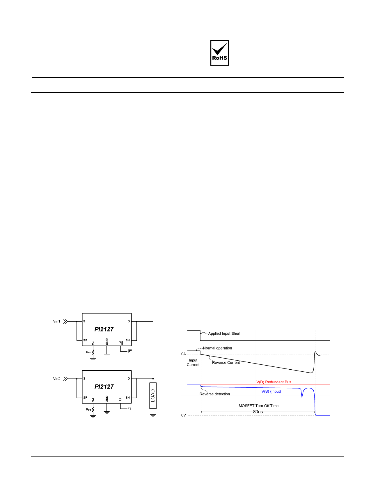
Figure 1: PI2127 High Side Active ORing
Picor Corporation • picorpower.com
Figure 2: PI2127 response time to an input short fault
condition
PI2127
Rev 1.3
Page 1 of 19
1 page 
Functional Description:
The PI2127 integrated Cool-ORing product takes
advantage of two different technologies combining
an 8.5mΩ on-state resistance (RDS(on)) N-channel
MOSFET with high density control circuitry. This
combination provides superior density, minimizing
PCB space to achieve an ideal ORing diode
function, significantly reducing power dissipation and
eliminating the need for heat sinking, while
minimizing design complexity.
The PI2127’s 8.5mΩ on-state resistance MOSFET
used in the conduction path enables a dramatic
reduction in power dissipation versus the
performance of a diode used in conventional ORing
applications due to its high forward voltage drop.
Due to the inherent characteristics of the MOSFET,
current will flow in the forward and reverse directions
while the gate remains above the gate threshold
voltage. Ideal ORing applications should not allow
reverse current flow, so the controller has to be
capable of very fast and accurate detection of
reverse current caused by input power source
failures, and very fast turn off of the gate of the
MOSFET. Once the gate voltage falls below the gate
threshold, the MOSFET is off and the body diode will
be reverse biased preventing reverse current flow
and subsequent excessive voltage droop on the
redundant bus.
Differential Amplifier:
The PI2127 integrates a high-speed low offset
voltage differential amplifier to sense the difference
between the Sense Positive (SP) pin voltage and
Sense Negative (SN) pin voltage with high sensitivity
to fault current. The amplifier output is connected to
the Reverse and Forward comparators.
Reverse Current Comparator: RVS
The reverse current comparator provides the critical
function in the controller, detecting negative voltage
caused by reverse current. Gate drive is enabled
when SP is 6mV higher than SN. When the SN pin
is 6mV higher than the SP pin, the reverse
comparator will force the gate discharge circuit to
turn off the MOSFET in typically 80ns and assert the
Fault ( FT ) low to report a fault condition.
The reverse comparator will hold the gate low until
the SP pin is 6mV higher than the SN pin. The
reverse comparator hysteresis is shown in Figure 3.
Figure 3: Reverse comparator hysteresis: VSP - VSN
Forward Voltage Comparator: FWD
The FWD comparator detects when a forward
voltage condition exists and SP is above 275mV
(typical) positive with respect to SN. When SP-SN is
more than 275mV, the FWD comparator will assert
the Fault ( FT ) low to report a fault condition.
Internal Voltage Regulator:
The PI2127 control circuitry and the gate driver are
biased through the S pin. An internal regulator
clamps the S voltage (VS-PG ) to 11.7V. The internal
regulator circuit has a comparator to monitor S input
with respect to the PG pin and pulls the MOSFET
GATE low when VS-PG is lower than the Under-
Voltage Threshold.
Fault Indication: FT
The FT pin is an open collector NPN that will be
pulled low during following fault conditions.
Typical Condition Indication of possible faults
1 Reverse: VSP-VSN ≤ -6mV
Input supply shorted
(MOSFET turned OFF)
2 Forward: VSP-VSN ≥ +275mV
Open FET, Gate short, Gate
open, or High current
(MOSFET turned ON)
3 Forward VSP-VSN ≤ +6mV
Shorted FET on power-up
(MOSFET turned OFF)
4 UVLO
4.5V < VS-PG<7.15V
Controller not ready
(MOSFET turned OFF)
Picor Corporation • picorpower.com
PI2127
Rev 1.3
Page 5 of 19
5 Page 
VS −PGMin : Controller minimum clamp voltage, 11V
IVC max : Controller maximum bias current, use
2.0mA
0.1mA : 0.1mA is added for margin
Example: 40V <VS-PG <50V
RPG
=
VS min − VS −PGMax
ICmax + 0.1mA
=
40V −12.5V
2.1mA
= 13.1kΩ
( )PdRPG
=
(VS −max
− VS −PGMin ) 2
RPG
=
50V −11V
13.1kΩ
2
= 116mW
Alternative Bias Circuit with Device Enable:
Constant current circuit
In a wide operating input voltage range the size of RPG
may be become large to support power dissipation. A
simple constant current circuit can be used instead of
RPG to reduce power dissipation and can be used as a
device enable.
As shown in Figure 20, the constant current circuit
consists of an NPN transistor (Q1), Zener diode DZ,
current limit resistor (RLIMIT) and Zener bias resistor
(RZ). RLIMIT and RZ can be very low power resistors
and Q1 is a signal transistor where its Collector-
Emitter Voltage (VCEO) is equal or greater than the
input operating voltage and supports 2.5mA at the
operating input voltage.
Figure 20: Constant current bias circuit
Pulling the Q1 base (EN) to the system return (RTN)
will turn off the transistor and the controller return (PG
pin) will float and eventually the MOSFET will be
turned off. An open collector device can be used to
enable and disable the PI2127.
The constant current circuit should guarantee current
greater than the PI2127 maximum Quiescent current
(IVC), 2.0mA.
RLIMIT can be calculated from the following equation:
RLIMIT
=
VZ
_
MIN − VBE
I VC _ MAX
(on)
Where:
VZ _ MIN : Minimum Zener diode voltage
VBE (on) : Q1 Base-Emitter On maximum voltage, for
default use VBE (on) =0.7V
Zener Diode Selection:
Select a Zener diode with a low reverse current
requirement to minimize RZ. Zener diodes with higher
break down voltage will have lower reverse current
and reduce Q1 collector current variation. Zener
diodes with a breakdown voltage of 6V and higher will
require low bias current for accurate voltage
breakdown.
RZ maximum value can be calculated with the
following equation:
Note that the surface mount resistors have limited
operating voltage capability. Be sure to pick a resistor
package that can meet the maximum operating
voltage (Vin).
RZ
=
Vin _ MIN
IZ +
− VZ _ MAX
I B _ MAX
Where:
Vin _ MIN : Min input voltage
VZ _ MAX : Zener diode maximum breakdown voltage
I Z : Zener diode required reverse current
I B _ MAX : Q1 required maximum base current which
calculated from the following equation:
I = hIB _ MAX
C _ MAX
FE _ MIN
I C _ MAX : Q1 maximum expected collector current.
hFE _ MIN : Q1 minimum gain.
Internal N-Channel MOSFET BVDSS:
The PI2127’s internal N-Channel MOSFET
breakdown voltage (BVDSS) is rated for 60V at 25°C
and will degrade to 55.5V at -40°C, refer to Figure 10.
Drain to source voltage should not exceed BVDSS in
nominal operation. During a fast switching transient
the MOSFET can tolerate voltages higher than its
BVDSS rating under avalanche conditions, refer to the
Absolute Maximum Ratings table.
In Active ORing applications when one of the input
power sources is shorted, a large reverse current is
Picor Corporation • picorpower.com
PI2127
Rev 1.3
Page 11 of 19
11 Page | ||
| Páginas | Total 19 Páginas | |
| PDF Descargar | [ Datasheet PI2127.PDF ] | |
Hoja de datos destacado
| Número de pieza | Descripción | Fabricantes |
| PI2121 | 24 Amp Full-Function Active ORing Solution | Vicor Corporation |
| PI2122 | 12Amp Active ORing Solution | Vicor Corporation |
| PI2123 | 15 Amp Full-Function Active ORing Solution | Vicor Corporation |
| PI2125 | 12 Amp Full-Function Active ORing Solution | Vicor Corporation |
| Número de pieza | Descripción | Fabricantes |
| SLA6805M | High Voltage 3 phase Motor Driver IC. |
Sanken |
| SDC1742 | 12- and 14-Bit Hybrid Synchro / Resolver-to-Digital Converters. |
Analog Devices |
|
DataSheet.es es una pagina web que funciona como un repositorio de manuales o hoja de datos de muchos de los productos más populares, |
| DataSheet.es | 2020 | Privacy Policy | Contacto | Buscar |