|
|
PDF XQR2V3000 Data sheet ( Hoja de datos )
| Número de pieza | XQR2V3000 | |
| Descripción | QPro Virtex-II 1.5V Radiation Hardened QML Platform FPGAs | |
| Fabricantes | Xilinx | |
| Logotipo |  |
|
Hay una vista previa y un enlace de descarga de XQR2V3000 (archivo pdf) en la parte inferior de esta página. Total 70 Páginas | ||
|
No Preview Available !
www.DataSheet.co.kr
0
R QPro Virtex-II 1.5V Radiation
Hardened QML Platform FPGAs
DS124 (v1.1) January 8, 2004
0 0 Product Specification
Summary of Radiation Hardened QPro™ Virtex™-II Features
• Industry First Radiation Hardened Platform FPGA
Solution
• Guaranteed total ionizing dose to 200K Rad(si)
• Latch-up immune to LET > 160 MeV-cm2/mg
• SEU in GEO upsets < 1.5E-6 per device day
achievable with recommended redundancy
implementation
• Certified to MIL-PRF-38535 (Qualified Manufacturer
Listing)
• Guaranteed over the full military temperature range
(–55° C to +125° C)
• Ceramic and Plastic Wire-Bond and Flip-Chip Grid
Array Packages
• IP-Immersion Architecture
- Densities from 1M to 6M system gates
- 300+ MHz internal clock speed (Advance Data)
- 622+ Mb/s I/O (Advance Data)
• SelectRAM™ Memory Hierarchy
- 2.5 Mb of dual-port RAM in 18 Kbit block
SelectRAM resources
- Up to 1 Mb of distributed SelectRAM resources
• High-Performance Interfaces to External Memory
- DRAM interfaces
· SDR/DDR SDRAM
· Network FCRAM
· Reduced Latency DRAM
- SRAM interfaces
· SDR/DDR SRAM
· QDR SRAM
- CAM interfaces
• Arithmetic Functions
- Dedicated 18-bit x 18-bit multiplier blocks
- Fast look-ahead carry logic chains
• Flexible Logic Resources
- Up to 67,584 internal registers/latches with Clock
Enable
- Up to 67,584 look-up tables (LUTs) or cascadable
16-bit shift registers
- Wide multiplexers and wide-input function support
- Horizontal cascade chain and sum-of-products
support
- Internal 3-state busing
• High-Performance Clock Management Circuitry
- Up to 12 DCM (Digital Clock Manager) modules
· Precise clock de-skew
· Flexible frequency synthesis
· High-resolution phase shifting
- 16 global clock multiplexer buffers
• Active Interconnect Technology
- Fourth generation segmented routing structure
- Predictable, fast routing delay, independent of
fanout
• SelectIO™-Ultra Technology
- Up to 824 user I/Os
- 19 single-ended and six differential standards
- Programmable sink current (2 mA to 24 mA) per
I/O
- Digitally Controlled Impedance (DCI) I/O: on-chip
termination resistors for single-ended I/O standards
- Differential Signaling
· 622 Mb/s Low-Voltage Differential Signaling I/O
(LVDS) with current mode drivers
· Bus LVDS I/O
· Lightning Data Transport (LDT) I/O with current
driver buffers
· Low-Voltage Positive Emitter-Coupled Logic
(LVPECL) I/O
· Built-in DDR input and output registers
- Proprietary high-performance SelectLink
Technology
· High-bandwidth data path
· Double Data Rate (DDR) link
· Web-based HDL generation methodology
• Supported by Xilinx Foundation Series™ and Alliance
Series™ Development Systems
- Integrated VHDL and Verilog design flows
- Compilation of 10M system gates designs
- Internet Team Design (ITD) tool
• SRAM-Based In-System Configuration
- Fast SelectMAP configuration
- IEEE 1532 support
- Partial reconfiguration
- Unlimited reprogrammability
- Readback capability
• 0.15 µm 8-Layer Metal Process with 0.12 µm
High-Speed Transistors
• 1.5V (VCCINT) Core Power Supply, Dedicated 3.3V
VCCAUX Auxiliary and VCCO I/O Power Supplies
• IEEE 1149.1 Compatible Boundary-Scan Logic Support
© 2004 Xilinx, Inc. All rights reserved. All Xilinx trademarks, registered trademarks, patents, and disclaimers are as listed at http://www.xilinx.com/legal.htm.
All other trademarks and registered trademarks are the property of their respective owners. All specifications are subject to change without notice.
DS124 (v1.1) January 8, 2004
Product Specification
www.xilinx.com
1-800-255-7778
1
Datasheet pdf - http://www.DataSheet4U.net/
1 page 
www.DataSheet.co.kr
R
QPro Virtex-II 1.5V Radiation Hardened QML Platform FPGAs
timing parameters, see QPro Virtex-II Switching Charac-
teristics, page 51.
Virtex-II devices have 16 global clock MUX buffers with up
to eight clock nets per quadrant. Each global clock MUX
buffer can select one of the two clock inputs and switch
glitch-free from one clock to the other. Each DCM block is
able to drive up to four of the 16 global clock MUX buffers.
Routing Resources
The IOB, CLB, block SelectRAM, multiplier, and DCM ele-
ments all use the same interconnect scheme and the same
access to the global routing matrix. Timing models are
shared, greatly improving the predictability of the perfor-
mance of high-speed designs.
There are a total of 16 global clock lines with eight available
per quadrant. In addition, 24 vertical and horizontal long
lines per row or column as well as massive secondary and
local routing resources provide fast interconnect. Virtex-II
buffered interconnects are relatively unaffected by net
fanout, and the interconnect layout is designed to minimize
crosstalk.
Horizontal and vertical routing resources for each row or
column include:
• 24 long lines
• 120 hex lines
• 40 double lines
• 16 direct connect lines (total in all four directions)
Boundary Scan
Boundary-scan instructions and associated data registers
support a standard methodology for accessing and config-
uring Virtex-II devices that complies with IEEE standards
1149.1 — 1993 and 1532. A system mode and a test mode
are implemented. In system mode, a Virtex-II device per-
forms its intended mission even while executing non-test
boundary-scan instructions. In test mode, boundary-scan
test instructions control the I/O pins for testing purposes.
The Virtex-II Test Access Port (TAP) supports BYPASS,
PRELOAD, SAMPLE, IDCODE, and USERCODE non-test
instructions. The EXTEST, INTEST, and HIGHZ test instruc-
tions are also supported.
Virtex-II Device/Package Combinations and Maximum I/O
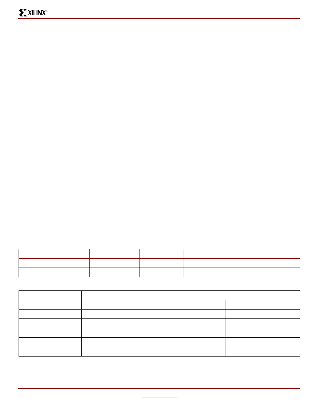
Wire-bond and flip-chip packages are available. Table 5
shows the maximum possible number of user I/Os in
wire-bond and flip-chip packages. Table 6 shows the num-
ber of available user I/Os for all device/package combina-
tions.
• FG denotes wire-bond fine-pitch Plastic BGA (1.00 mm
pitch).
• BG denotes wire-bond standard Plastic BGA (1.27 mm
pitch).
• CG denotes wire-bond fine-pitch Hermetic Ceramic
Column Grid Array (1.27 mm pitch).
• CF denotes flip-chip fine-pitch non-Hermetic Ceramic
Column Grid Array (1.00 mm pitch).
The number of I/Os per package include all user I/Os except
the 15 control pins (CCLK, DONE, M0, M1, M2, PROG_B,
PWRDWN_B, TCK, TDI, TDO, TMS, HSWAP_EN, DXN,
DXP, and RSVD) and VBATT.
Table 5: Package Information
Package
Pitch (mm)
Size (mm)
FG456
1.00
23 x 23
BG575
1.27
31 x 31
BG728 & CG717
1.27
35 x 35
CF1144
1.00
35 x 35
Table 6: Virtex-II Device/Package Combinations and Maximum Number of Available I/Os
Available I/Os
Package
XQR2V1000
XQR2V3000
FG456
324
-
BG575
328
-
BG728
-
516
CG717
-
516
CF1144
-
-
Notes:
1. The BG728 and CG717 packages are pinout (footprint) compatible.
2. The CF1144 is pinout (footprint) compatible with the FF1152.
XQR2V6000
-
-
-
-
824
DS124 (v1.1) January 8, 2004
Product Specification
www.xilinx.com
1-800-255-7778
5
Datasheet pdf - http://www.DataSheet4U.net/
5 Page 
www.DataSheet.co.kr
R
QPro Virtex-II 1.5V Radiation Hardened QML Platform FPGAs
The optional weak-keeper circuit is connected to each out-
put. When selected, this circuit monitors the voltage on the
pad and weakly drives the pin High or Low. If the pin is con-
nected to a multiple-source signal, the weak-keeper holds
the signal in its last state if all drivers are disabled. Maintain-
ing a valid logic level in this way eliminates bus chatter.
Pull-up or pull-down resistors override the weak-keeper cir-
cuit.
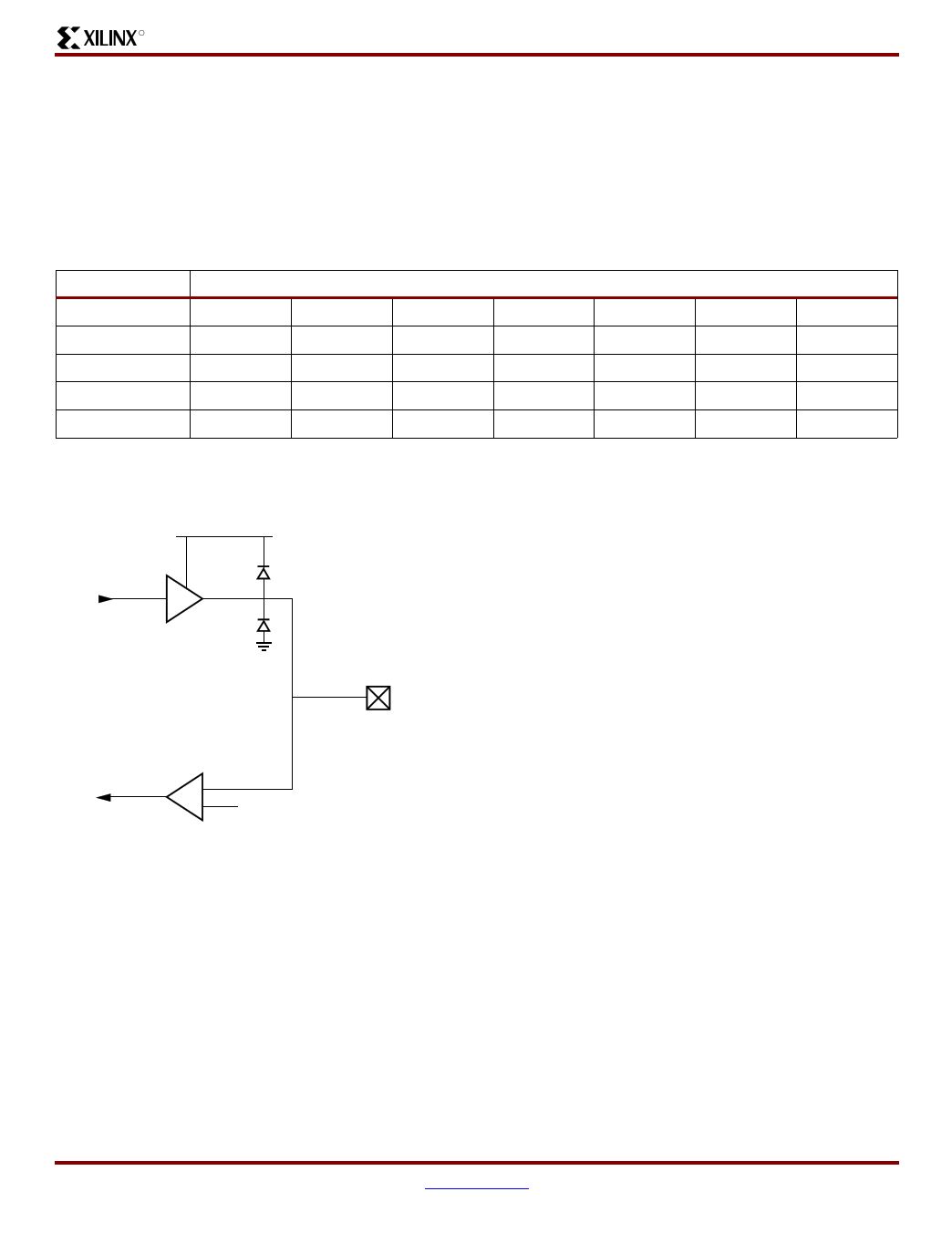
LVTTL sinks and sources current up to 24 mA. The current
is programmable for LVTTL and LVCMOS SelectI/O-Ultra
standards (see Table 10). Drive-strength and slew-rate con-
trols for each output driver minimize bus transients. For
LVDCI and LVDCI_DV2 standards, drive strength and
slew-rate controls are not available.
Table 10: LVTTL and LVCMOS Programmable Currents (Sink and Source)
SelectI/O-Ultra
Programmable Current (Worst-Case Guaranteed Minimum)
LVTTL
2 mA
4 mA
6 mA
8 mA
12 mA
16 mA
LVCMOS33
2 mA
4 mA
6 mA
8 mA
12 mA
16 mA
LVCMOS25
2 mA
4 mA
6 mA
8 mA
12 mA
16 mA
LVCMOS18
2 mA
4 mA
6 mA
8 mA
12 mA
16 mA
LVCMOS15
2 mA
4 mA
6 mA
8 mA
12 mA
16 mA
24 mA
24 mA
24 mA
n/a
n/a
Figure 7 shows the SSTL2, SSTL3, and HSTL configura-
tions. HSTL can sink current up to 48 mA. (HSTL IV)
OBUF
VCCO
Clamp
Diode
PAD
VREF
VCCAUX = 3.3V
VCCINT = 1.5V
DS031_24_100900
Figure 7: SSTL or HSTL SelectI/O-Ultra Standards
All pads are protected against damage from electrostatic
discharge (ESD) and from over-voltage transients. Virtex-II
devices use two memory cells to control the configuration of
an I/O as an input. This is to reduce the probability of an I/O
configured as an input from flipping to an output when sub-
jected to a single event upset (SEU) in space applications.
Prior to configuration, all outputs not involved in configura-
tion are forced into their high-impedance state. The
pull-down resistors and the weak-keeper circuits are inac-
tive. The dedicated pin HSWAP_EN controls the pull-up
resistors prior to configuration. By default, HSWAP_EN is
driven High, which disables the pull-up resistors on user I/O
pins. When HSWAP_EN is driven Low, the pull-up resistors
are activated on user I/O pins.
All Virtex-II IOBs support IEEE 1149.1 compatible bound-
ary-scan testing.
Input Path
The Virtex-II IOB input path routes input signals directly to
internal logic and/or through an optional input flip-flop or
latch, or through the DDR input registers. An optional delay
element at the D-input of the storage element eliminates
pad-to-pad hold time. The delay is matched to the internal
clock-distribution delay of the Virtex-II device, and when
used, ensures that the pad-to-pad hold time is zero.
Each input buffer can be configured to conform to any of the
low-voltage signaling standards supported. In some of
these standards the input buffer utilizes a user-supplied
threshold voltage, VREF. The need to supply VREF imposes
constraints on which standards can be used in the same
bank. See I/O Banking description below.
Output Path
The output path includes a 3-state output buffer that drives
the output signal onto the pad. The output and/or the 3-state
signal can be routed to the buffer directly from the internal
logic or through an output/3-state flip-flop or latch, or
through the DDR output/3-state registers.
Each output driver can be individually programmed for a
wide range of low-voltage signaling standards. In most sig-
naling standards, the output High voltage depends on an
externally supplied VCCO voltage. The need to supply VCCO
imposes constraints on which standards can be used in the
same bank. See I/O Banking description below.
I/O Banking
Some of the I/O standards described above require VCCO
and VREF voltages. These voltages are externally supplied
DS124 (v1.1) January 8, 2004
Product Specification
www.xilinx.com
1-800-255-7778
11
Datasheet pdf - http://www.DataSheet4U.net/
11 Page | ||
| Páginas | Total 70 Páginas | |
| PDF Descargar | [ Datasheet XQR2V3000.PDF ] | |
Hoja de datos destacado
| Número de pieza | Descripción | Fabricantes |
| XQR2V3000 | QPro Virtex-II 1.5V Radiation Hardened QML Platform FPGAs | Xilinx |
| Número de pieza | Descripción | Fabricantes |
| SLA6805M | High Voltage 3 phase Motor Driver IC. |
Sanken |
| SDC1742 | 12- and 14-Bit Hybrid Synchro / Resolver-to-Digital Converters. |
Analog Devices |
|
DataSheet.es es una pagina web que funciona como un repositorio de manuales o hoja de datos de muchos de los productos más populares, |
| DataSheet.es | 2020 | Privacy Policy | Contacto | Buscar |
