|
|
PDF AT76C401 Data sheet ( Hoja de datos )
| Número de pieza | AT76C401 | |
| Descripción | Dual-mode CMOS Integrated Imager | |
| Fabricantes | ATMEL Corporation | |
| Logotipo |  |
|
Hay una vista previa y un enlace de descarga de AT76C401 (archivo pdf) en la parte inferior de esta página. Total 27 Páginas | ||
|
No Preview Available !
www.DataSheet.co.kr
Features
• SVGA Resolution, Active CMOS Imager Sensor for Highest Quality Images
• CIF-sized Sub-sample Mode for Easy Video Conferencing
• Stand-alone Operation – Need Only to Supply One 26.6MHz Clock
• Ultra-low Fixed Pattern Noise
• Triple 10-bit ADCs and Column-based CDS for Highest Readout Speed
• High Fill Factor and Sensitivity without Microlens Distortions
• Full 10-bit Data Width Digital Interface for Simple, Fast Transfer
• Easy Register-based Programming of Modes
• Region of Interest Image Scan Control for Digital Zoom and Metering
• On-board Color Offset and Gain Control
• Option for Full Timing and Scan Control through External FPGA
• Direct Interface to 8- or 16-bit-based Microprocessor Bus
• Full Power Control – Low-power Viewfinder Mode
• Internal Timing Mode Only Covered in this Datasheet
Description
The Atmel AT76C401 is a complete imager system on one IC that has been designed
to give high-quality images using an easy interface and simple operation to reduce
overall system cost and time-to-market.
The core is a pixel array of 1281 x 480 rectangular active pixels with a high physical fill
factor of 43% (without micro-lenses). A vertical stripe RGB pastel color filter is used
with individual column-correlated double-sampling (CDS) correction circuitry to pro-
duce an exceptionally low level of fixed-pattern image noise (FPN). Individual color
gain and offset controls followed by a triple 10-bit analog-to-digital converter further
ensure an even color response in the digitized images.
All timing and voltages are generated internally from a single 3.3V voltage rail and
master clock, but the option is available to take control of every aspect of scan timing
externally in an FPGA if the user requires the modes of operation extended for
advanced imaging.
Pre-programmed modes are available for full-resolution still- and motion-imaging with
exposures of 1 µs to 1 second, as well as for a sub-sampled CIF-sized image suitable
for the quality and data rates required for video conferencing.
Region of Interest mode additionally allows the user to define on a frame-by-frame
basis the area of the imager to be read, enabling easy digital zone or complex multi-
spot metering routines utilizing an external FPGA.
The interface resembles a standard microprocessor bus with a 4-bit address bus and
the full image data width of 10 bits operating in a slave mode. When a local processor
is not available, the device will stream data in a host mode out to a parallel interface
with minimal flow control.
Dual-mode
CMOS
Integrated
Imager
AT76C401
Preliminary
Rev. 1174A–03/00
1
Datasheet pdf - http://www.DataSheet4U.net/
1 page 
www.DataSheet.co.kr
AT76C401
Table 2. Physical and Electrical Parameters (Continued)
Parameter
Measurement
Noise
130
Saturation
100
Peak Quantum Efficiency
21
Full Well Capacity
95000
Programmable Gain Range
2x - 48x
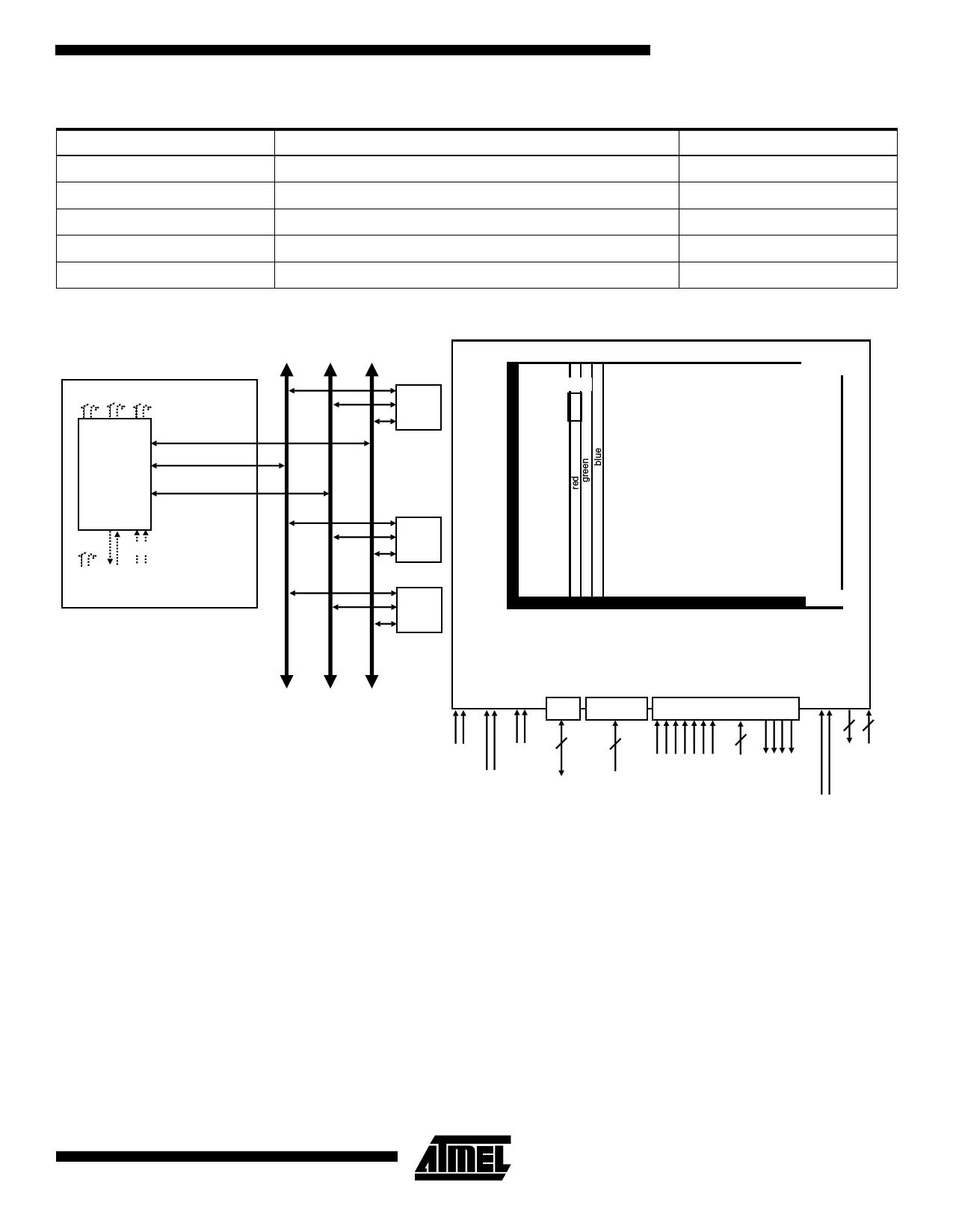
Figure 3. Image Format
Data Address Control
AVDD DVDD PVDD
AGND DGND PGND
nWR, nRD, nCS, MC,
FR, ROW_B, ROW_R,
ROI, nFS, nLS, nPX,
ACK
Image
Acquisition
D00 - D09
Die
Betty
A00 - A03
u-controller
1 pixel
(test)
480
pixels
6.0um
12um
DAR, G, B
VA SA
IAR, G, B
Analog
PIX ASET
DRAM
removable
memory/
interface
9 pixels
(dark)
(0, 0)
21 pixels
(dark)
Units
e-
uA
%
e-
(1305, 490)
Image Sensor Array
e.g. 1281 + 2 pixels
(1304, 0)
1 pixel
(test)
A00 - A23
D00 - D15
nWR, nRD, nCS,
MC, FR, ROW_B,
ROW_R, ROI, nFS,
nLS, nPX, ACK
Data
Port
Vdd Vss
padring
Vdd Vss
digital
10
Vdd Vss
analog
Register
Value
Address
Port
Control
Port
33
4
2
analog analog
master clock
mode pixel synch out
frame reset
select line synch
Register
Address
row blanking
row read
chip select
read
frame synch
acknowledge
analog pixel
write
trim test
in
bias
5
Datasheet pdf - http://www.DataSheet4U.net/
5 Page 
www.DataSheet.co.kr
AT76C401
Full Motion
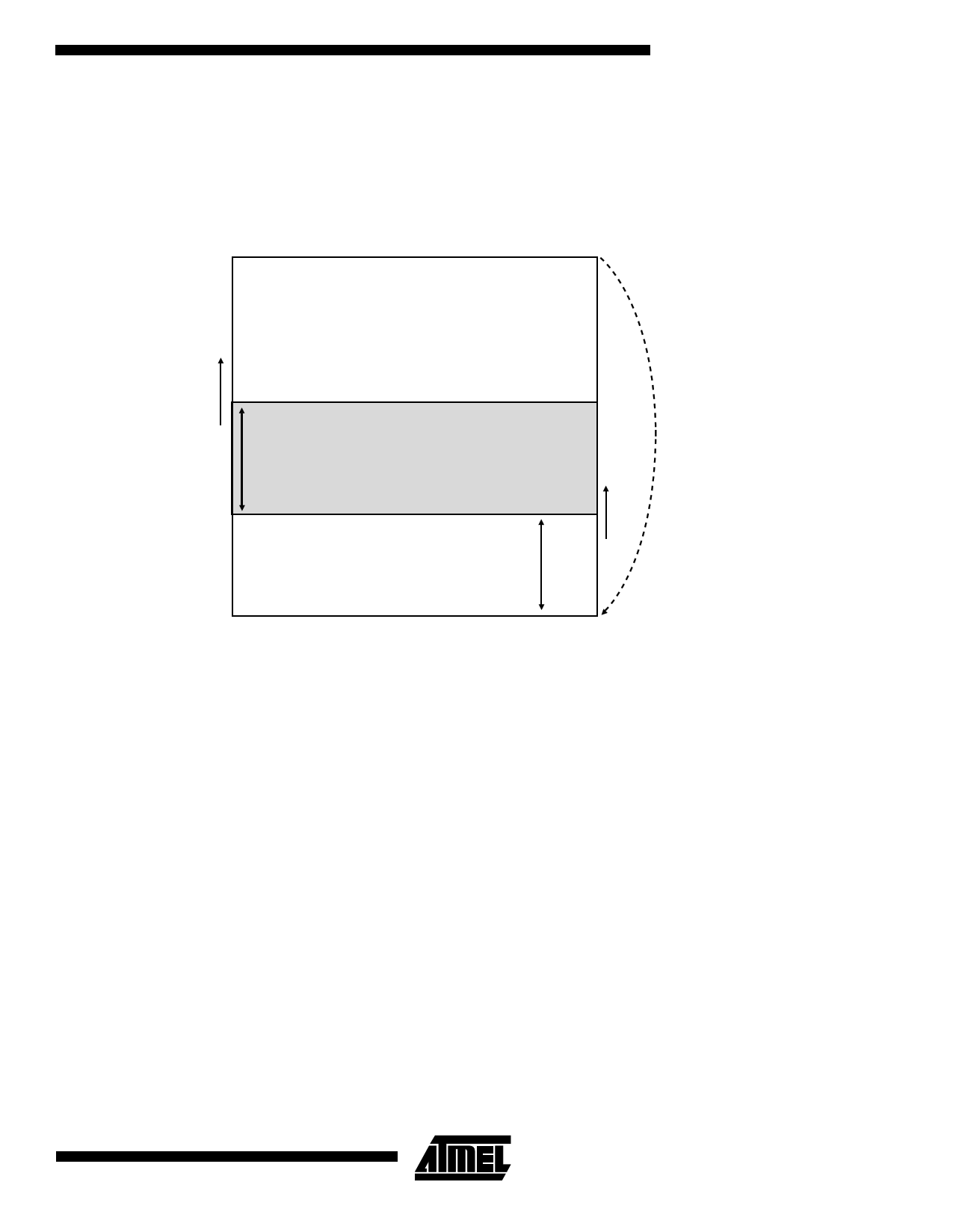
For continuous image acquisition, exposure is controlled
using a moving blade electronic shutter the width of which
is written into the Image Sensor Logic (IL) register before a
frame is exposed.
Figure 11. Moving Blade Shutter
Stop Row
Reset Row wraps to Start Row
before Row Read reaches Stop Row
Moving Blade Shutter
*(f = 1/T)
Reset Row
Nreset
Nread
Number of Rows
"Exposure" in
INL Register
Exposure
Zone
Indeterminate
Exposure
*(f = 1/T)
Read Row
Start Row
* must be identical and constant
T = "Row B Strobe Period"
A single frame is acquired by strobing Frame Reset (FR) to
reset to the top of the frame. FR does not reset the full
frame of pixels in this mode. After the reset operation is
ACK’d, the user then moves the shutter across the imager
by strobing RowB high for each row. This rate should be
calculated such that the datastream produced by the
imager does not exceed the maximum interface bandwidth
and requires to be at a constant rate so that the exposure
does not vary across the image.
The exposure can be calculated as:
Exposure(ms) = Row B strobe period × no. of rows in register INL
The data rate can be calculated as:
Data Rate = (1 ⁄ Row B strobe period) × 3 × ’x’ Block Size
The exact interface bandwidth will most likely depend
heavily upon how the 10-bit data is coded into bytes. Users
requiring only 8-bit images may opt to drop the 2 LSBs.
For the first frame following a Frame Reset or nCS, valid
data is not available until the programmed exposure period
for the first line has been reached. During this period, the
last n (where n is the number of lines of the exposure) lines
of the imager are read out followed by the nFS line going
low. As these lines will have been reset at an indeterminate
time, the data obtained will be random. To establish the
true start of the image, the user should flush the TX buffer
following the first frame sync (nFS) and not attempt to
count lines as the period will not be constant. The first
frame of the image will thus appear to be much shorter/
smaller than the programmed region of interest being the
width of the exposure.
11
Datasheet pdf - http://www.DataSheet4U.net/
11 Page | ||
| Páginas | Total 27 Páginas | |
| PDF Descargar | [ Datasheet AT76C401.PDF ] | |
Hoja de datos destacado
| Número de pieza | Descripción | Fabricantes |
| AT76C401 | Dual-mode CMOS Integrated Imager | ATMEL Corporation |
| AT76C402 | USB and Parallel Port Mode Integrated CMOS Imager | ATMEL Corporation |
| Número de pieza | Descripción | Fabricantes |
| SLA6805M | High Voltage 3 phase Motor Driver IC. |
Sanken |
| SDC1742 | 12- and 14-Bit Hybrid Synchro / Resolver-to-Digital Converters. |
Analog Devices |
|
DataSheet.es es una pagina web que funciona como un repositorio de manuales o hoja de datos de muchos de los productos más populares, |
| DataSheet.es | 2020 | Privacy Policy | Contacto | Buscar |
