|
|
|
PDF APL5932A Data sheet ( Hoja de datos )
| Número de pieza | APL5932A | |
| Descripción | Ultra Low Dropout (0.3V Typical) Linear Regulator | |
| Fabricantes | ANPEC | |
| Logotipo | ||
Hay una vista previa y un enlace de descarga de APL5932A (archivo pdf) en la parte inferior de esta página. Total 18 Páginas | ||
|
No Preview Available !
WWWWWW. W.10.100Y0.0Y0.YC.OCMOM.OM.T.WTWW WWWWWWW.1W.10.100Y0.YC0.YC.OCMOM. M.T.WTWAPL5932A/B/C/D
WWWWW.1 .100Y.YC.COM.T.TW WWWWW.10.100Y.C.OCOM.T.WTW3A, Ultra Low Dropout (0.3V Typical) Linear Regulator
WWWWW.10.1000Y.COMOM.TWW WWWWW.1000Y0Y.COMOM.TWWFeatures
General Description
WWW .100Y.C OM.T W W WW.1 00Y.C OM.T W• Ultra Low Dropout
W W 0Y.C M.T W W.1 Y.C .T- 0.3V (Typical) at 3A Output Current
WW W.10 Y.CO .TW WW .100 .COM .TW• Low ESR output Capasitor (Milti-layer Chip
W W 00 OM W W 0Y MCapasitors (MLCC)) Applicable
T W W W.1 0Y.C M.T WW W.10 Y.CO .TW• 0.8V Reference Voltage
M.T WW W.10 Y.CO .TW WW .100 .COM .TW• High Output Accuracy
W W 00 OM W W 0Y M- ±1.5% Over Line, Load, and Temperature Range
M.T W W.1 Y.C .T WW .10 .CO .TW• Fast Transient Response
O M.TW WW W.100 Y.COM .TW WWW .100Y OM W• Adjustable Output Voltage
O W W 00 OM W W 0Y.C M.T• Power-On-Reset Monitoring on Both VCNTL and
C M.T W W.1 Y.C .T WW .10 .CO .TWVIN Pins
Y.CO .TW WW .100 OM W WW 00Y OM W• Internal Soft-Start
OM W WW 00Y.C OM.T W W W.1 0Y.C M.T• Current-Limit and Short Current-Limit Protections
0Y.C M.T W W.1 Y.C .T WW .10 .CO .T• Thermal Shutdown with Hysteresis
Y.CO .TW WW .100 OM W WW 00Y OM• Open-Drain VOUT Voltage Indicator (POK)
100 OM W WW 00Y.C OM.T W W W.1 0Y.C M• Low Shutdown Quiescent Current (< 30µA )
0Y.C M.T W W.1 Y.C .T WW .10 .CO• BuiltinShutdown/EnableControlwithfloatinghigh/
.10 O W W 00 OM W W 0Ylow Function
W 00Y.C OM.T W W W.1 0Y.C M.T WW W.10 Y.CO• Simple SOP-8P Package with Exposed Pad
W.1 0Y.C M.T WW W.10 Y.CO .TW WW .100 .C• Lead Free and Green Devices Available
W .10 O W W 00 OM W W 0Y(RoHS Compliant)
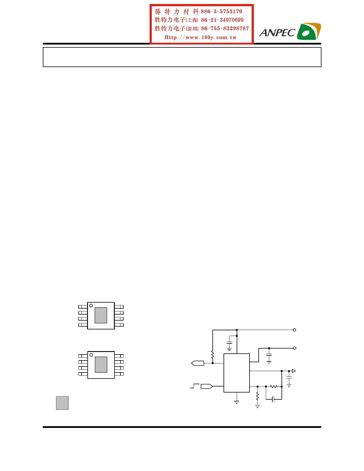
WWWW.100Y0.YC.COMM.T.TW WWWWW.1 .100Y.YC.COM.T.TW WWWWW.10.100YPin Configuration
The APL5932A/B/C/D is a 3A ultra low dropout linear
regulator. The IC needs two supply voltages, one is a
control voltage (VCNTL) for the control circuitry, the other is
a main supply Voltage(VIN) for power conversion, to re-
duce power dissipation and provide extremely low drop-
out voltage.
The APL5932A/B/C/D integrates many functions. A Power-
On-Reset (POR) circuit monitors both supply voltages on
VCNTL and VIN pins to prevent erroneous operations. The
functions of thermal shutdown and current-limit protect
the device against thermal and current over-loads. A POK
indicates that the output voltage status with a delay time
set internally. It can control other converter for power
sequence. APL5932A/B/C/D can be enabled by other
power systems. Pulling and holding the EN voltage be-
low 0.4V or ENB above 1.2V will shuts off the output.
The APL5932A/B/C/D is available in a SOP-8P package
which features small size as SOP-8 and an Exposed
Pad to reduce the junction-to-case resistance to extend
power range of applications.
Applications
• Motherboards, VGA Cards
• Notebook PCs
• Add-in Cards
WW W.10 0Y.CO M.TW WW W.100 Y.COM .TW WWW .10POK 1
W 0 O W 0 M WEN 2
W W.1 Y.C .T WW .10 O W WVIN 3
WWWW.10000Y.COMOM.TWW WWWW.100Y0.YC.COMM.T.TW WWWWW.1VCNTL 4
APL5932A/B
SOP-8P
(Top View)
8 GND
7 FB
6 VOUT
5 NC
W WW.1 00Y.C OM.T W WW W.10 0Y.CO M.TW WWPOK 1
W W.1 Y.C .T WW .10 .CO .TW WENB 2
0 M W Y WVIN 3
WWWWWW.10.100Y.YC.OCOM.T.WTW WWWWW.10.1000Y.C.OCMOM.T.WTW WVCNTL 4
APL5932C/D
SOP-8P
(Top View)
8 GND
7 FB
6 VOUT
5 NC
Simplified Application Circuit
VCNTL
POK
EN
Enable
VCNTL
POK
VIN
VOUT
APL5932
A/B/C/D
EN FB
GND
VIN
VOUT
WW W.100 Y.COM .TW WWW .100Y OM W= Exposed Pad
.C .T(connected to ground plane for better heat dissipation)
Optional
WW .100 OM W WW 00Y OM WANPEC reserves the right to make changes to improve reliability or manufacturability without notice, and
W Y.C .T W .1 .C .Tadvise customers to obtain the latest version of relevant information to verify before placing orders.
WW W.100 Y.COM .TW WWW .100Y .COM .TWCopyright © ANPEC Electronics Corp.
W 00 OM W W 0Y MRev. A.1 - Aug., 2011
1
www.anpec.com.tw
WWWWW.1 .100Y0.YC.COMM.T.TW WWWWWW.10.100Y0.YC.OCOMM.T.WTWFreeDatasheethttp://www.datasheetlist.com/
1 page 
WMWOWWYCT10WWW.MW.0OWW.YCT10WWW.MWW.0OWW.YCT10WWW.MWW.0O.WW.YCT10WWW.MWW.0O.WW.YCT110WWW0.MWW.0O.WW.YCT1100WWW0.MWW.0O.YWW.YCATRCT1100eWo.WWy0.MWW.0O.vYpWWP.YCT1.y10p0W.WrWA0.MWLW.0O.YCWiW.iYCg.T11c010hW5.W11223344W0O.MWW.0Oa.tYCW1122334W3333444445505050505-.YCT10505050510..........00000000009©02468024680lWA000000000.WMW0O.MWW-.0O.YCWuW0.5YCAOT130DVV10g0D0NWVV.WMWCOr..0O.MWWr.0O.YpCW,PWCOoNU2.YCoT1NTUT10Ep20L-pTWTe=.0WMW2C.0O.LoMW0=AW.0O.=YoCW0W..5TYC=25Tu11r.1u501E50.WJt515.MVWa/t..0O.MWlWOW.0O.2uYCVWVVWeJ.TYCOVT1VVuu1nt0oc0C0oBWuCnt.MWt1cil.0O.pMWW.tN0lO.YCrtWucW.TYpCnt1tuaTT1ota1i0ru/Lit0ogWonr.gMWtVg=.0O.CMWWen.0O.2eYnCWWi.CTYeCTCTcTC1un5310TNvJ0usJT1Wr.vTt.MTCWe31r.0O=.Msr=W-We..0O.LYCseWJr/.5TYCLm.VC.T1em5=n2=2.10hi0OonWp5t5T5.mOMW5.0,O.-MDpWWt.e0Or.T0YCWJu,aTYCVIuTpC1CeriOJ=0Itat0OWU.tT=rp.Mr2Wt.0O.pvM-WUTWa.O.uY2CJWuTYCCT1as74Tu(1t=r0AW2e(ut050.WtA.MW51.0cO.)MCWWr.O.YCW(C)TYCC2oeT1uCCt20W5uW2..MrW)1e.0O.MW5rW.O.YCrW.CTCr05Te1e0r0WWnW.MWn.0OMWWi.O.YCWtTtTs101W3WW.M2WWt3.0OMWW..YCW5TiT10WcWW.MWW.0O.MWW..YCWsT1T150WWW.MWW.0O.WW..YCWT1T10WWW0.MWW.0O.WW.YCWT1100WWW0.MWW.0O.YWW.YCT1100W000000000.WW0.MWW11223344.0O.YC....W.....W.YC888787787T05050505511000000111100090990900000000000W.W.........W8648046022.MW567890123W-.0O.YCWW.Y5C0T110D0VV0W.WW0O.MWWOCr.0O.YCWW.YCoNUT110TT0pW-L.WMW200O=.MWW.0O.uYCWJ=W.YC5.RT1SJ51t1u005Weu..WMhVWJn.0O.8MVWW.0O.YCWfWOn.uYCooVceT110nc0u0lrtWVr.tWMcWti.0O.ttMeWWa.0O.YCoCpWW1ti.TYCCinT1Noguo1n0T0Wuctnne.TMWL.0O.MWWW.0O.TYCC2WeWrJ=.TYCTvT1Tre5=10u0eVe5sWem1.MrW.0O.MmW2VWno..r0Om.YCW.W.TYCe55T1pOtVlp10Tnt0-pW5ee.CMaWLJCut.0O.MWW.0O.e0,YNCWrWr=.wTYgCitaT1TIamr10pOLTe0t-waWt.uMWU=u.0O.MJW2Wui.0O.tYCWrTvw.TYtC=utTe173r1(0sv0.eCArW.51.M(Wa3..0O.MCseWW.0O.YC)W2uCTYVCn.oT150Cr)p02W.rMW1.0O.)MWeW.C.O.eYCW50TYCTc1n000.W.MtWc.0O.MWW.O.YCWoTYCT101mW.MW23.0O.MWW.O.YCW.5TCtT10wW.MW.0OMWW.O.YCWTT10W.MW.0OMWW..YCWTT10W.MWF.0OMWrWe..YCeWDTaT1tas0heeWt.hMWt.0OtWpW..:YCW//TwwT1w0.daWta.sMWh.0OeWWe.YCtWliTst.1com0/W.MW.0OWW.YCT1
5 Page 
WWWWWW. W.10.100Y0.0Y0.YC.OCMOM.OM.T.WTWW WWWWWWW.1W.10.100Y0.YC0.YC.OCMOM. M.T.WTWAPL5932A/B/C/D
WWWWW.1 .100Y.YC.COM.T.TW WWWWW.10.100Y.C.OCOM.T.WTWFunction Description
WW W.100 Y.COM .TW WWW .100Y .COM .TWPower-On-Reset
WW W.100 Y.COM .TW WWW .100Y .COM .TWA Power-On-Reset (POR) circuit monitors both of supply
W 00 OM W W 0Y Mvoltages on VCNTL and VIN pins to prevent wrong logic
W W.1 Y.C .T WW .10 .CO .TWcontrols. The POR function initiates a soft-start process
W WW .100 OM W WW 00Y OM Wafter both of the supply voltages exceed their rising POR
W Y.C .T W .1 .C .Tvoltage thresholds during powering on. The POR func-
TW WW .100 OM W WW 00Y OM Wtion also pulls low the POK voltage regardless of the
W WW 00Y.C OM.T W W W.1 0Y.C M.Toutput status when one of the supply voltages falls below
M.T W W.1 Y.C .T WW .10 .CO .TWits falling POR voltage threshold.
M.TW WW W.100 Y.COM .TW WWW .100Y OM WInternal Soft-Start
O .TW WW .100 OM W WW 00Y.C OM.T WAn internal soft-start function controls rise rate of the out-
M W Y.C .T W .1 .C .Tput voltage to limit the current surge during start-up. The
CO .TW WW .100 OM W WW 00Y OM Wtypical soft-start interval is about 0.6ms.
Y.COM .TW WWW .100Y.C OM.T W W WW.1 00Y.C OM.T WOutput Voltage Regulation
OM W WW 00Y.C OM.T W W W.1 0Y.C M.TAn error amplifier working with a temperature-compen-
0Y.C M.T W W.1 Y.C .T WW .10 .CO .Tsated 0.8V reference and an output NMOS regulates out-
O W W 00 OM W W 0Y Mput to the preset voltage. The error amplifier is designed
0Y.C M.T W W.1 Y.C .T WW .10 .COwith high bandwidth and DC gain provides very fast tran-
10 Y.CO .TW WW .100 OM W WW 00Y OMsient response and less load regulation. It compares the
00 OM W W 0Y.C M.T W W.1 Y.Creference with the feedback voltage and amplifies the dif-
W.1 0Y.C M.T WW W.10 Y.CO .TW WW .100 .COference to drive the output NMOS which provides load
.10 O W W 00 OM W W 0Ycurrent from VIN to VOUT.
WW .100Y.C OM.T W W WW.1 00Y.C OM.T W WW W.10 0Y.CCurrent-Limit Protection
W 0Y.C M.T W W.1 Y.C .T WW .10The APL5932A/B/C/D monitors the current flowing through
WW W.10 Y.CO .TW WW .100 OM W WW 00Ythe output NMOS and limits the maximum current to pre-
W 00 OM W W 0Y.C M.T W W.1vent load and APL5932A/B/C/D from damages during cur-
W W.1 0Y.C M.T WW W.10 Y.CO .TW WW .10rent overload conditions.
WW W.10 0Y.CO M.TW WW W.100 Y.COM .TW WWW .1Short Current-Limit Protection
WW W.10 Y.CO .TW WW .100 OM W WWThe short current-limit function reduces the current-limit
W 00 OM W W 0Y.C M.T W Wlevel down to 0.9A (typical) when the voltage on FB pin
W W.1 Y.C .T WW .10 .CO .TW Wfalls below 0.2V (typical) during current overload or short-
W 00 OM W W 0Y M Wcircuit conditions.
W W.1 Y.C .T WW .10 .CO .TW WThe short current-limit function is disabled for success-
WW .100 OM W WW 00Y OM W Wful start-up during soft-start interval.
Thermal Shutdown
A thermal shutdown circuit limits the junction tempera-
ture of APL5932A/B/C/D. When the junction temperature
exceeds +170oC, a thermal sensor turns off the output
NMOS, allowing the device to cool down. The regulator
regulates the output again through initiation of a new soft-
start process after the junction temperature cools by 50oC,
resulting in a pulsed output during continuous thermal
overload conditions. The thermal shutdown is designed
with a 50oC hysteresis to lower the average junction tem-
perature during continuous thermal overload conditions,
extending lifetime of the device.
For normal operation, the device power dissipation should
be externally limited so that junction temperatures will
not exceed +125οC.
Enable Control
The APL5932A/B/C/D has a dedicated enable pin (EN/
ENB). A logic low/high signal applied to this pin shuts
down the output. Following a shutdown, a logic high/low
signal re-enables the output through initiation of a new
turn on delay and soft-start cycle. When left open, this pin
is pulled up/down by an internal current source (3µA
typical) to enable normal operation. It’s not necessary to
use an external transistor to save cost.
Power-OK and Delay
The APL5932A/B/C/D indicates the status of the output
voltage by monitoring the feedback voltage (VFB) on FB
pin. As the V rises and reaches the rising Power-OK
FB
voltage threshold (VTHPOK), an internal delay function starts
to work. At the end of the delay time, the IC turns off the
internal NMOS of the POK to indicate the output is ok. As
the VFB falls and reaches the falling Power-OK voltage
threshold, the IC turns on the NMOS of the POK ( after a
debounce time of 10µs typical ).
WWWWWWWWWWW.10W.100W.Y10.0.YC10.0YC0.OYC.MOYC.M.OCTM.OTM.WT.WT.WTW WWWWWWWWWW.1WW.10W.100.Y10.0.YC10.0YC0.OYC.MOC.M.OCTM.OTM.WT.WT.WTW WCopyright © ANPEC Electronics Corp.
WWWWWW.10.1000Y0.YC.OCMOMM.T.WTW WWWWWWW.10.100Y0Y0.YC.OCMOMM.T.WTWRev. A.1 - Aug., 2011
11
www.anpec.com.tw
Free Datasheet http://www.datasheetlist.com/
11 Page | ||
| Páginas | Total 18 Páginas | |
| PDF Descargar | [ Datasheet APL5932A.PDF ] | |
Hoja de datos destacado
| Número de pieza | Descripción | Fabricantes |
| APL5932A | Ultra Low Dropout (0.3V Typical) Linear Regulator | ANPEC |
| APL5932B | Ultra Low Dropout (0.3V Typical) Linear Regulator | ANPEC |
| APL5932C | Ultra Low Dropout (0.3V Typical) Linear Regulator | ANPEC |
| APL5932D | Ultra Low Dropout (0.3V Typical) Linear Regulator | ANPEC |
| Número de pieza | Descripción | Fabricantes |
| SLA6805M | High Voltage 3 phase Motor Driver IC. |
Sanken |
| SDC1742 | 12- and 14-Bit Hybrid Synchro / Resolver-to-Digital Converters. |
Analog Devices |
|
DataSheet.es es una pagina web que funciona como un repositorio de manuales o hoja de datos de muchos de los productos más populares, |
| DataSheet.es | 2020 | Privacy Policy | Contacto | Buscar |