|
|
PDF AT25DF021 Data sheet ( Hoja de datos )
| Número de pieza | AT25DF021 | |
| Descripción | 2-Megabit 2.3-volt or 2.7-volt Minimum SPI Serial Flash Memory | |
| Fabricantes | Adesto Technologies | |
| Logotipo |  |
|
Hay una vista previa y un enlace de descarga de AT25DF021 (archivo pdf) en la parte inferior de esta página. Total 30 Páginas | ||
|
No Preview Available !
Features
• Single 2.3V - 3.6V or 2.7V - 3.6V Supply
• Serial Peripheral Interface (SPI) Compatible
– Supports SPI Modes 0 and 3
• 66 MHz Maximum Operating Frequency
– Clock-to-Output (tV) of 6 ns Maximum
• Flexible, Optimized Erase Architecture for Code + Data Storage Applications
– Uniform 4-Kbyte Block Erase
– Uniform 32-Kbyte Block Erase
– Uniform 64-Kbyte Block Erase
– Full Chip Erase
• Individual Sector Protection with Global Protect/Unprotect Feature
– Four Sectors of 64 Kbytes Each
• Hardware Controlled Locking of Protected Sectors via WP Pin
• 128-Byte Programmable OTP Security Register
• Flexible Programming
– Byte/Page Program (1 to 256 Bytes)
• Fast Program and Erase Times
– 1.0 ms Typical Page Program (256 Bytes) Time
– 50 ms Typical 4-Kbyte Block Erase Time
– 250 ms Typical 32-Kbyte Block Erase Time
– 450 ms Typical 64-Kbyte Block Erase Time
• Automatic Checking and Reporting of Erase/Program Failures
• JEDEC Standard Manufacturer and Device ID Read Methodology
• Low Power Dissipation
– 7 mA Active Read Current (Typical at 20 MHz)
– 15 μA Deep Power-Down Current (Typical)
• Endurance: 100,000 Program/Erase Cycles
• Data Retention: 20 Years
• Complies with Full Industrial Temperature Range
• Industry Standard Green (Pb/Halide-free/RoHS Compliant) Package Options
– 8-lead SOIC (150-mil Wide)
– 8-pad Ultra Thin DFN (5 x 6 x 0.6 mm)
2-Megabit
2.3-volt or
2.7-volt
Minimum
SPI Serial Flash
Memory
AT25DF021
(Not Recommended
for New Designs)
1. Description
The AT25DF021 is a serial interface Flash memory device designed for use in a wide
variety of high-volume consumer based appl ications in which program code is shad-
owed from Flash memory into embedded or external RAM for execution. The flexible
erase architecture of the AT25DF021, with its erase granularity as small as 4 Kbytes,
makes it ideal for data storage as well, eliminating the need for additional data storage
EEPROM devices.
3677F–DFLASH–5/2013
http://www.Datasheet4U.com
1 page 
AT25DF021
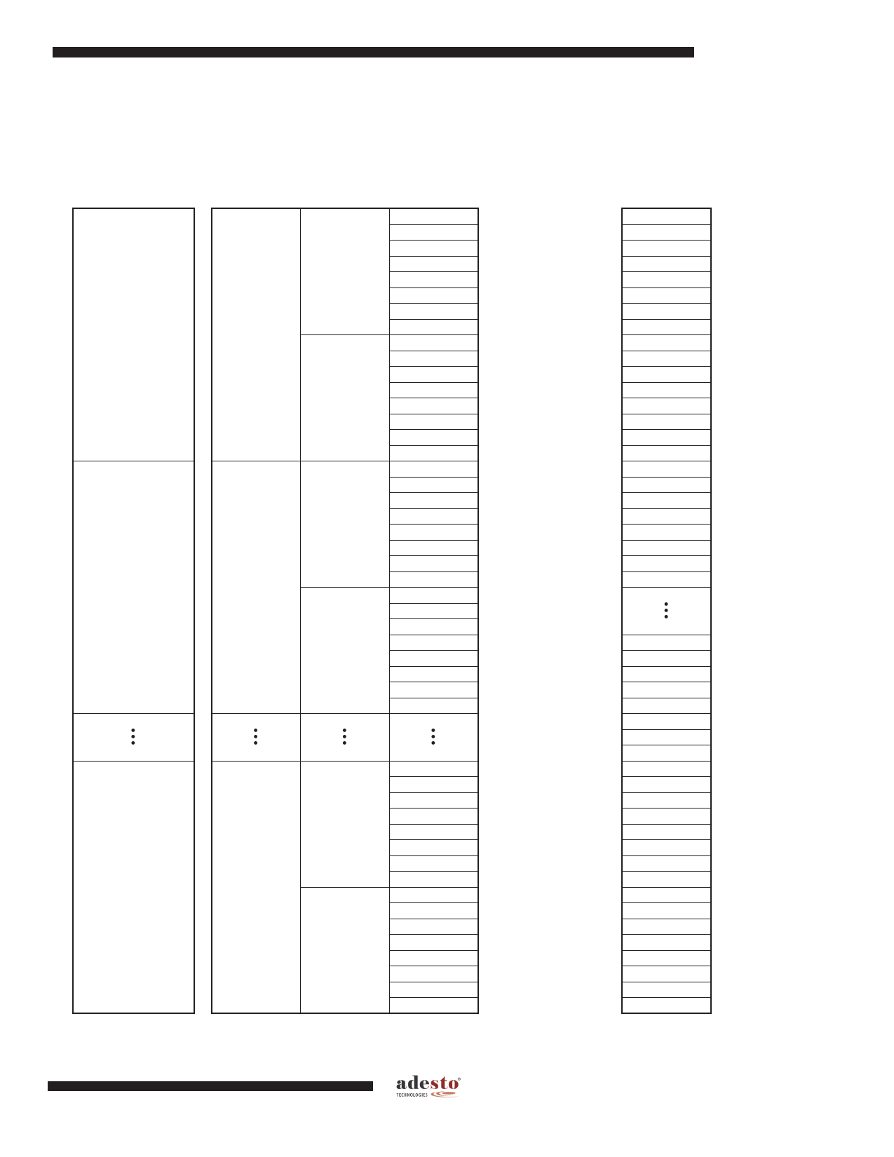
Figure 4-1.
Memory Architecture Diagram
Block Erase Detail
Internal Sectoring for
Sector Protection
Function
64KB
(Sector 3)
64KB
(Sector 2)
64KB
32KB
4KB
Block Erase
Block Erase
Block Erase
(D8h Command) (52h Command) (20h Command)
Block Address
Range
64KB
32KB
32KB
64KB
32KB
32KB
4KB 03FFFFh – 03F000h
4KB 03EFFFh – 03E000h
4KB 03DFFFh – 03D000h
4KB 03CFFFh – 03C000h
4KB 03BFFFh – 03B000h
4KB 03AFFFh – 03A000h
4KB 039FFFh – 039000h
4KB 038FFFh – 038000h
4KB 037FFFh – 037000h
4KB 036FFFh – 036000h
4KB 035FFFh – 035000h
4KB 034FFFh – 034000h
4KB 033FFFh – 033000h
4KB 032FFFh – 032000h
4KB 031FFFh – 031000h
4KB 030FFFh – 030000h
4KB 02FFFFh – 02F000h
4KB 02EFFFh – 02E000h
4KB 02DFFFh – 02D000h
4KB 02CFFFh – 02C000h
4KB 02BFFFh – 02B000h
4KB 02AFFFh – 02A000h
4KB 029FFFh – 029000h
4KB 028FFFh – 028000h
4KB 027FFFh – 027000h
4KB 026FFFh – 026000h
4KB 025FFFh – 025000h
4KB 024FFFh – 024000h
4KB 023FFFh – 023000h
4KB 022FFFh – 022000h
4KB 021FFFh – 021000h
4KB 020FFFh – 020000h
64KB
(Sector 0)
64KB
32KB
32KB
4KB 00FFFFh – 00F000h
4KB 00EFFFh – 00E000h
4KB 00DFFFh – 00D000h
4KB 00CFFFh – 00C000h
4KB 00BFFFh – 00B000h
4KB 00AFFFh – 00A000h
4KB 009FFFh – 009000h
4KB 008FFFh – 008000h
4KB 007FFFh – 007000h
4KB 006FFFh – 006000h
4KB 005FFFh – 005000h
4KB 004FFFh – 004000h
4KB 003FFFh – 003000h
4KB 002FFFh – 002000h
4KB 001FFFh – 001000h
4KB 000FFFh – 000000h
Page Program Detail
1-256 Byte
Page Program
(02h Command)
Page Address
Range
256 Bytes
256 Bytes
256 Bytes
256 Bytes
256 Bytes
256 Bytes
256 Bytes
256 Bytes
256 Bytes
256 Bytes
256 Bytes
256 Bytes
256 Bytes
256 Bytes
256 Bytes
256 Bytes
256 Bytes
256 Bytes
256 Bytes
256 Bytes
256 Bytes
256 Bytes
256 Bytes
256 Bytes
03FFFFh – 03FF00h
03FEFFh – 03FE00h
03FDFFh – 03FD00h
03FCFFh – 03FC00h
03FBFFh – 03FB00h
03FAFFh – 03FA00h
03F9FFh – 03F900h
03F8FFh – 03F800h
03F7FFh – 03F700h
03F6FFh – 03F600h
03F5FFh – 03F500h
03F4FFh – 03F400h
03F3FFh – 03F300h
03F2FFh – 03F200h
03F1FFh – 03F100h
03F0FFh – 03F000h
03EFFFh – 03EF00h
03EEFFh – 03EE00h
03EDFFh – 03ED00h
03ECFFh – 03EC00h
03EBFFh – 03EB00h
03EAFFh – 03EA00h
03E9FFh – 03E900h
03E8FFh – 03E800h
256 Bytes
256 Bytes
256 Bytes
256 Bytes
256 Bytes
256 Bytes
256 Bytes
256 Bytes
256 Bytes
256 Bytes
256 Bytes
256 Bytes
256 Bytes
256 Bytes
256 Bytes
256 Bytes
256 Bytes
256 Bytes
256 Bytes
256 Bytes
256 Bytes
256 Bytes
256 Bytes
256 Bytes
0017FFh – 001700h
0016FFh – 001600h
0015FFh – 001500h
0014FFh – 001400h
0013FFh – 001300h
0012FFh – 001200h
0011FFh – 001100h
0010FFh – 001000h
000FFFh – 000F00h
000EFFh – 000E00h
000DFFh – 000D00h
000CFFh – 000C00h
000BFFh – 000B00h
000AFFh – 000A00h
0009FFh – 000900h
0008FFh – 000800h
0007FFh – 000700h
0006FFh – 000600h
0005FFh – 000500h
0004FFh – 000400h
0003FFh – 000300h
0002FFh – 000200h
0001FFh – 000100h
0000FFh – 000000h
3677F–DFLASH–5/2013
5
5 Page 
AT25DF021
If the address specified by A23-A0 points to a memory location within a sector that is in the pro-
tected state, then the Block Erase command will not be executed, and the device will return to
the idle state once the CS pin has been deasserted.
The WEL bit in the Status Register will be reset back to the logical “0” state if the erase cycle
aborts due to an incomplete address being sent, the CS pin being deasserted on uneven byte
boundaries, or because a memory location within the region to be erased is protected.
While the device is executing a successful erase cycle, the Status Register can be read and will
indicate that the device is busy. For faster throughput, it is recommended that the Status Regis-
ter be polled rather than waiting the tBLKE time to determine if the device has finished erasing. At
some point before the erase cycle completes, the WEL bit in the Status Register will be reset
back to the logical “0” state.
The device also incorporates an intelligent erase algorithm that can detect when a byte location
fails to erase properly. If an er ase error occurs, it will be indicat ed by the EPE bit in the Status
Register.
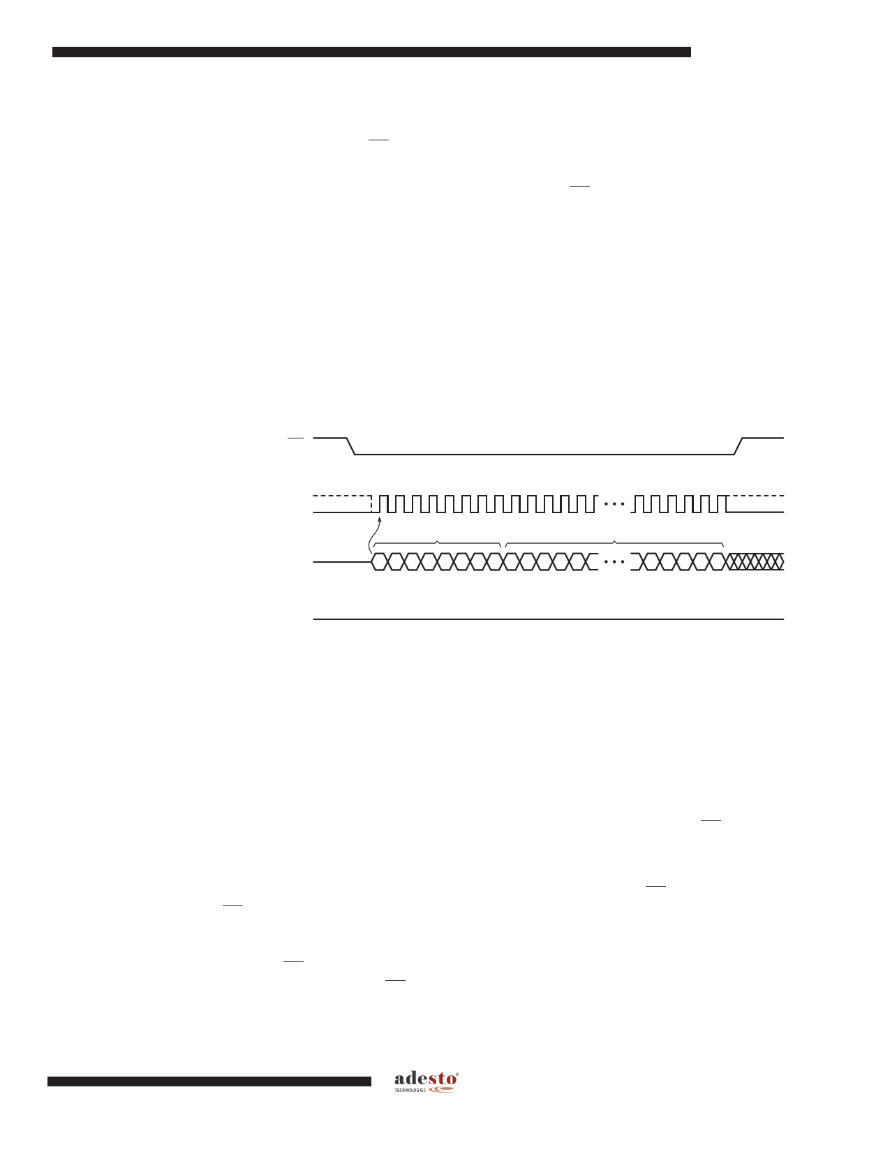
Figure 8-3. Block Erase
CS
SCK
SI
0 1 2 3 41 5 67
81 9 0 11 2
26 27 28 29 30 31
OPCODE
CCCCCCCC
MSB
ADDRESS BITS A23-A0
AAAAAA
MSB
AAA
AAA
SO
HIGH-IMPEDANCE
8.3 Chip Erase
The entire memory array can be erased in a single operation by using the Chip Erase command.
Before a Chip Erase command can be started, the Write Enable command must have been pre-
viously issued to the device to set the WEL bit of the Status Register to a logical “1” state.
Two opcodes, 60h and C7h, can be used for the Chip Erase command. There is no difference in
device functionality when utilizing the two opcodes, so they can be used interchangeably. To
perform a Chip Erase, one of the two opcodes (60h or C7h) must be clocked into the device.
Since the entire memory array is to be erased, no address bytes need to be clocked into the
device, and any data clocked in after the opcode will be ignored. When the CS pin is deasserted,
the device will erase the entire memory array. The erasing of the device is internally self-timed
and should take place in a time of tCHPE.
The complete opcode must be clocked into the device before the CS pin is deasserted, and the
CS pin must be deasserted on an even byte boundary (multiples of eight bits); otherwise, no
erase will be performed. In addition, if any sector of the memory array is in the protected state,
then the Chip Erase command will not be executed, and the device will return to the idle state
once the CS pin has been deasserted. The WEL bit in the Status Register will be reset back to
the logical “0” state if the CS pin is deasserted on uneven byte boundaries or if a sector is in the
protected state.
3677F–DFLASH–5/2013
11
11 Page | ||
| Páginas | Total 30 Páginas | |
| PDF Descargar | [ Datasheet AT25DF021.PDF ] | |
Hoja de datos destacado
| Número de pieza | Descripción | Fabricantes |
| AT25DF021 | 2-Megabit 2.3-volt or 2.7-volt Minimum SPI Serial Flash Memory | Adesto Technologies |
| Número de pieza | Descripción | Fabricantes |
| SLA6805M | High Voltage 3 phase Motor Driver IC. |
Sanken |
| SDC1742 | 12- and 14-Bit Hybrid Synchro / Resolver-to-Digital Converters. |
Analog Devices |
|
DataSheet.es es una pagina web que funciona como un repositorio de manuales o hoja de datos de muchos de los productos más populares, |
| DataSheet.es | 2020 | Privacy Policy | Contacto | Buscar |
