|
|
|
PDF HGTG40N60B3 Data sheet ( Hoja de datos )
| Número de pieza | HGTG40N60B3 | |
| Descripción | UFS Series N-Channel IGBT | |
| Fabricantes | Harris | |
| Logotipo | ||
Hay una vista previa y un enlace de descarga de HGTG40N60B3 (archivo pdf) en la parte inferior de esta página. Total 6 Páginas | ||
|
No Preview Available !
HGTG40N60B3S E M I C O N D U C T O R
PRELIMINARY
May 1995
70A, 600V, UFS Series N-Channel IGBT
Features
• 70A, 600V at TC = +25oC
• Square Switching SOA Capability
• Typical Fall Time - 160ns at +150oC
• Short Circuit Rating
• Low Conduction Loss
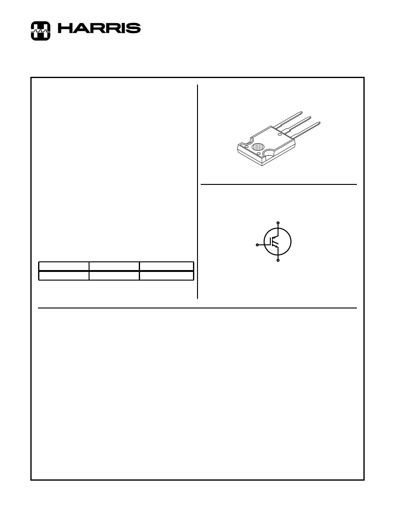
Package
JEDEC STYLE TO-247
E
C
G
Description
The HGTG40N60B3 is a MOS gated high voltage switching
device combining the best features of MOSFETs and bipolar
transistors. The device has the high input impedance of a
MOSFET and the low on-state conduction loss of a bipolar
transistor. The much lower on-state voltage drop varies only
moderately between +25oC and +150oC.
Terminal Diagram
N-CHANNEL ENHANCEMENT MODE
The IGBT is ideal for many high voltage switching
applications operating at moderate frequencies where low
conduction losses are essential, such as: AC and DC motor
controls, power supplies and drivers for solenoids, relays
and contactors.
PACKAGING AVAILABILITY
PART NUMBER
PACKAGE
BRAND
HGTG40N60B3
TO-247
G40N60B3
NOTE: When ordering, use the entire part number.
Formerly Developmental Type TA49052
C
G
E
Absolute Maximum Ratings TC = +25oC, Unless Otherwise Specified
Collector-Emitter Voltage . . . . . . . . . . . . . . . . . . . . . . . . . . . . . . . . . . . . . . . . . . . . BVCES
Collector-Gate Voltage, RGE = 1MΩ. . . . . . . . . . . . . . . . . . . . . . . . . . . . . . . . . . . . BVCGR
Collector Current Continuous
At TC = +25oC (Package Limited) . . . . . . . . . . . . . . . . . . . . . . . . . . . . . . . . . . . . . IC25
At TC = +110oC . . . . . . . . . . . . . . . . . . . . . . . . . . . . . . . . . . . . . . . . . . . . . . . . . . . IC110
Collector Current Pulsed (Note 1) . . . . . . . . . . . . . . . . . . . . . . . . . . . . . . . . . . . . . . . . ICM
Gate-Emitter Voltage Continuous. . . . . . . . . . . . . . . . . . . . . . . . . . . . . . . . . . . . . . . VGES
Gate-Emitter Voltage Pulsed . . . . . . . . . . . . . . . . . . . . . . . . . . . . . . . . . . . . . . . . . . VGEM
Switching Safe Operating Area at TC = +150oC. . . . . . . . . . . . . . . . . . . . . . . . . . . .SSOA
Power Dissipation Total at TC = +25oC . . . . . . . . . . . . . . . . . . . . . . . . . . . . . . . . . . . . PD
Power Dissipation Derating TC > +25oC . . . . . . . . . . . . . . . . . . . . . . . . . . . . . . . . . . . . . .
Operating and Storage Junction Temperature Range . . . . . . . . . . . . . . . . . . . . . TJ, TSTG
Maximum Lead Temperature for Soldering . . . . . . . . . . . . . . . . . . . . . . . . . . . . . . . . . . TL
Short Circuit Withstand Time (Note 2) at VGE = 15V . . . . . . . . . . . . . . . . . . . . . . . . . . tSC
Short Circuit Withstand Time (Note 2) at VGE = 10V . . . . . . . . . . . . . . . . . . . . . . . . . . tSC
NOTE:
1. Repetitive Rating: Pulse width limited by maximum junction temperature.
2. VCE(PK) = 360V, TC = +125oC, RGE = 25Ω.
HGTG40N60B3
600
600
70
40
330
±20
±30
160A at 0.8 BVCES
290
2.33
-40 to +150
260
2
10
UNITS
V
V
A
A
A
V
V
W
W/oC
oC
oC
µs
µs
CAUTION: These devices are sensitive to electrostatic discharge. Users should follow proper ESD Handling Procedures.
Copyright © Harris Corporation 1995
9-3
File Number 3943
1 page 
HGTG40N60B3
Typical Performance Curves (Continued)
TJ = +150oC, TC = +75oC, VGE = +15V, RG = 3Ω, L = 100µH
200
100
50
20
10 fMAX1 = 0.05/(tD(OFF)I + tD(ON)I)
fMAX2 = (PD - PC)/(EON + EOFF)
5 PD = ALLOWABLE DISSIPATION
PC = CONDUCTION DISSIPATION
2 (DUTY FACTOR = 50%)
RθJC = 0.43oC/W
1
10 20 30
50
70
ICE, COLLECTOR-EMITTER CURRENT (A)
100
FIGURE 13. OPERATING FREQUENCY AS A FUNCTION OF
COLLECTOR-EMITTER CURRENT
200 TC = +150oC, VGE = 15V, RG = 3Ω, L = 45µH
160
120
80
40
0
0 100 200 300 400 500 600
VCE, COLLECTOR-EMITTER VOLTAGE (V)
FIGURE 14. SWITCHING SAFE OPERATING AREA
100
0.5
0.2
10-1 0.1
0.05
0.02
0.01
10-2
10-5
SINGLE PULSE
10-4
10-3
PD
NOTES:
t1
t2
DUTY FACTOR, D = t1/t2
PEAK TJ = (PD X ZθJC X RθJC) + TC
10-2
10-1
100
t1, RECTANGULAR PULSE DURATION (s)
FIGURE 15. IGBT NORMALIZED TRANSIENT THERMAL IMPEDANCE, JUNCTION TO CASE
Test Circuit and Waveforms
101
RG = 3Ω
L = 100µH
RHRP3060
+
- VDD = 480V
VGE
VCE
ICE
90%
EOFF
10%
EON
90%
10%
tD(OFF)I tFI
tRI
tD(ON)I
FIGURE 16. INDUCTIVE SWITCHING TEST CIRCUIT
FIGURE 17. SWITCHING TEST WAVEFORMS
9-7
5 Page | ||
| Páginas | Total 6 Páginas | |
| PDF Descargar | [ Datasheet HGTG40N60B3.PDF ] | |
Hoja de datos destacado
| Número de pieza | Descripción | Fabricantes |
| HGTG40N60B3 | UFS Series N-Channel IGBT | Fairchild Semiconductor |
| HGTG40N60B3 | 70A/ 600V/ UFS Series N-Channel IGBT | Intersil Corporation |
| HGTG40N60B3 | UFS Series N-Channel IGBT | Harris |
| Número de pieza | Descripción | Fabricantes |
| SLA6805M | High Voltage 3 phase Motor Driver IC. |
Sanken |
| SDC1742 | 12- and 14-Bit Hybrid Synchro / Resolver-to-Digital Converters. |
Analog Devices |
|
DataSheet.es es una pagina web que funciona como un repositorio de manuales o hoja de datos de muchos de los productos más populares, |
| DataSheet.es | 2020 | Privacy Policy | Contacto | Buscar |