|
|
|
PDF CH7308A-TF-TR Data sheet ( Hoja de datos )
| Número de pieza | CH7308A-TF-TR | |
| Descripción | LVDS Transmitter | |
| Fabricantes | Chrontel | |
| Logotipo | ||
Hay una vista previa y un enlace de descarga de CH7308A-TF-TR (archivo pdf) en la parte inferior de esta página. Total 22 Páginas | ||
|
No Preview Available !
Chrontel
CH7308
CH7308 SDVO1 LVDS Transmitter
Features
General Description
• Single/Dual LVDS Transmitter up to 140Mpixels/s
(CH7308A)
• Single/Dual LVDS Transmitter up to 165Mpixels/s
(CH7308B)
• Support resolutions up to 1600x1200 (1920x1200
with reduced blanking)
• LVDS low jitter PLL accepts spread spectrum input
• LVDS 18-bit and 24-bit outputs
• 2D dither engine
• Panel protection and power sequencing
• High-speed SDVO1 serial (1G~2Gbps) AC-coupled
differential RGB inputs
• Low voltage interface support to graphics device
• Programmable power management
• Fully programmable through serial port
• Configuration through OpCodes1
• Complete Windows driver support
• Boundary scan support
• Offered in a 64-pin LQFP package
1Intel Proprietary
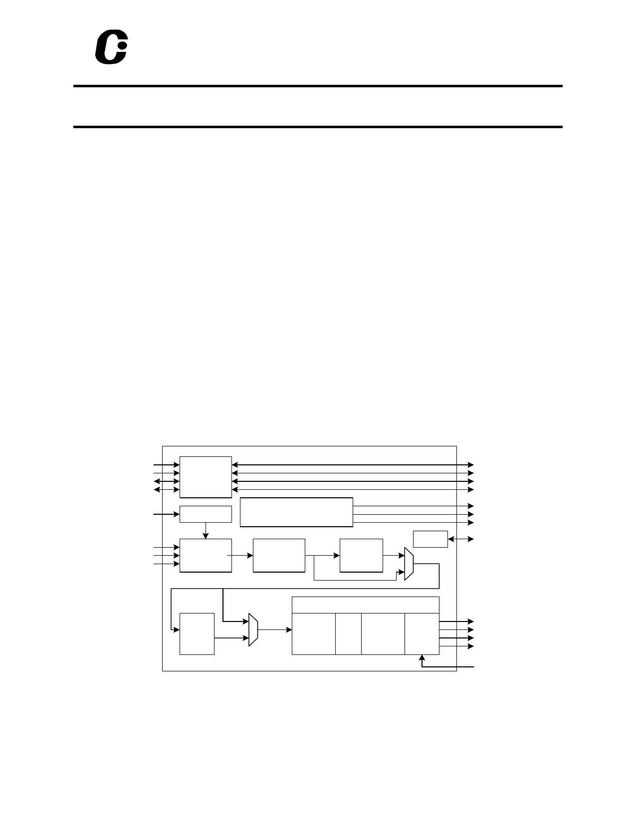
The CH7308 is a display controller device, which accepts
digital graphics input signals, upscales, encodes, and transmits
data through an LVDS transmitter to a LCD panel. This
device accepts one channel of RGB data over three pairs of
serial data ports.
The LVDS Transmitter includes a low jitter PLL to generate a
high frequency serialized clock and all circuitry required to
upscale, encode, serialize and transmit data. The CH7308A
supports a maximum single channel pixel rate of 140MP/s
while the CH7308B supports a maximum pixel rate of
165MP/s. The minimum dual channel pixel rate is 100MP/s.
The LVDS transmitter includes a panel fitting up-scaler and a
programmable dither function to support 18-bit LCD panels.
Data is encoded into commonly used formats, including those
specified in the OpenLDI and SPWG specifications.
Serialized data is outputted on three to eight differential
channels.
RESET*
AS
SPC
SPD
SDVO_CLK(+/-)
SDVO_R(+/-)
SDVO_G(+/-)
SDVO_B(+/-)
Serial Port/
Power
Control
Clock Driver
Data Latch,
Serial To
Parallel
STALL(+/-) Generator/
Power Sequencing
SDVO
Character
Decoder
Up-Scaler
XTAL
SC_PROM
SD_PROM
SC_DDC
SD_DDC
SDVO_STALL(+/-)
ENAVDD
ENABKL
XI/FIN, XO
Dither
LVDS PLL
LVDS
Encoder
FIFO
LVDS
Serializer
LVDS
Driver
Figure 1: Functional Block Diagram
LDC[3:0],LDC*[3:0]
LL1C,LL1C*
LDC[7:4],LDC*[7:4]
LL2C,LL2C*
VSWING
201-0000-064 Rev. 2.3, 9/22/2008
1
1 page 
CHRONTEL
CH7308
Pin#
51, 52, 54,
55, 57, 58
60, 61
47, 48
36, 37
17, 18
33, 39, 42,
45, 34, 40,
43, 46
20, 23, 26,
29, 21, 24,
27, 30
32
14
15
16, 49
13, 31
19, 25, 38,
44
22, 28, 35,
41
56, 62
53, 59
3
8
Type
In
In
Out
Out
Out
Out
Out
In
In
Out
Power
Power
Power
Power
Power
Power
Power
Power
Symbol
SDVO_R+/-
SDVO_G+/-
SDVO_B+/-
SDVO_CLK+/-
SDVO_STALL+/-
LL1C, LL1C*
LL2C, LL2C*
LDC[3:0], LDC*[3:0]
Description
SDVO Data Channel Inputs
These pins accept 3 AC-coupled differential pair of inputs from
the digital video port of a graphics controller. These 3 pairs of
inputs can be R, G, B. The differential p-p input voltage has a
maximum value of 1.2V, with a minimum value of 175mV.
Differential Clock Input associated with SDVO Data Channel
(SDVO_R+/-, SDVO_G+/-, SDVO_B+/-)
The range of this clock pair is 100~200MHz. For specific pixel
rates in specific modes, this clock pair will run at an integer
multiple of the pixel rate. Refer to section 2.1.2 for details.
Stall Signal Pair associated with SDVO Data Channel
(SDVO_R+/-, SDVO_G+/-, SDVO_B+/-)
This differential pair is used as a stall indication for a VGA
controller, which is capable of driving out SDVO_R+/-,
SDVO_G+/-, SDVO_B+/- data. When toggling between 100MHz
and 200MHz, the stall indication state is asserted (‘1’ value);
when not toggling at all the state is de-asserted (‘0’ value). The
differential p-p output voltage has a maximum value of 1.2V, with
a minimum value of 175mV.
LVDS Differential Clock Channel 1
LVDS Differential Clock Channel 2
LVDS Differential Data[3:0]
LDC[7:4], LDC*[7:4] LVDS Differential Data [7:4]
VSWING
XI/FIN
XO
DVDD
DGND
LVDD
LGND
AVDD
AGND
AVDD_PLL
AGND_PLL
LVDS Swing Control
This pin sets the swing level of the LVDS outputs. A 2.4KOhm
resistor should be connected between this pin and LGND using
short and wide traces.
Crystal Input/External Reference Input
A parallel resonant 14.31818 MHz crystal (+/-1000 ppm) should
be attached between this pin and XO. Alternatively, an external
CMOS compatible clock may be used to drive the XI/FIN input.
Crystal Output
A parallel resonant 14.31818 MHz crystal (+/-1000 ppm) should
be attached between this pin and XI/FIN. However, if an external
CMOS clock is attached to XI/FIN, XO should be left open.
Digital Supply Voltage (2.5V)
Digital Ground
LVDS Supply Voltage (3.3V)
LVDS Ground
Analog Supply Voltage (2.5V)
Analog Ground
LVDS PLL Supply Voltage (3.3V)
LVDS PLL Ground
201-0000-064 Rev. 2.3, 9/22/2008
5
5 Page 
CHRONTEL
CH7308
2.7.1 NAND Tree Test
CH7308 provides “NAND TREE Testing” to verify IO cell functions at the PC board level. This test will check the
interconnect between the chip’s I/O and the printed circuit board for faults (soldering, bent leads, open printed
circuit board traces, etc.). The NAND tree test is a simple serial logic which turns all IO cell signals to input mode,
connects all inputs with NAND gates as shown in Figure 6 and switches each signal to high or low according to the
sequence in Table 7. The test results are then passed out of pin 48 (SDVO_STALL-). This test is enabled when the
BSCAN pin (pin 63) is set to “1”.
Figure 5: NAND Tree Connection
Testing Sequence
Set BSCAN = 1; (internal weak pull low)
Set all signals listed in Table 7 to 1.
Set all signals listed in Table 7 to 0, toggle one by one with a suggested time period of 200 ns.
Pin 48 will change its value each time an input value changed.
201-0000-064 Rev. 2.3, 9/22/2008
11
11 Page | ||
| Páginas | Total 22 Páginas | |
| PDF Descargar | [ Datasheet CH7308A-TF-TR.PDF ] | |
Hoja de datos destacado
| Número de pieza | Descripción | Fabricantes |
| CH7308A-TF-TR | LVDS Transmitter | Chrontel |
| Número de pieza | Descripción | Fabricantes |
| SLA6805M | High Voltage 3 phase Motor Driver IC. |
Sanken |
| SDC1742 | 12- and 14-Bit Hybrid Synchro / Resolver-to-Digital Converters. |
Analog Devices |
|
DataSheet.es es una pagina web que funciona como un repositorio de manuales o hoja de datos de muchos de los productos más populares, |
| DataSheet.es | 2020 | Privacy Policy | Contacto | Buscar |