|
|
PDF MX25L512C Data sheet ( Hoja de datos )
| Número de pieza | MX25L512C | |
| Descripción | 512K-BIT [x 1] CMOS SERIAL FLASH | |
| Fabricantes | Macronix International | |
| Logotipo |  |
|
Hay una vista previa y un enlace de descarga de MX25L512C (archivo pdf) en la parte inferior de esta página. Total 30 Páginas | ||
|
No Preview Available !
MX25L512C
MX25L512C
DATASHEET
P/N: PM1469
REV. 1.2, OCT. 06, 2009
1
1 page 
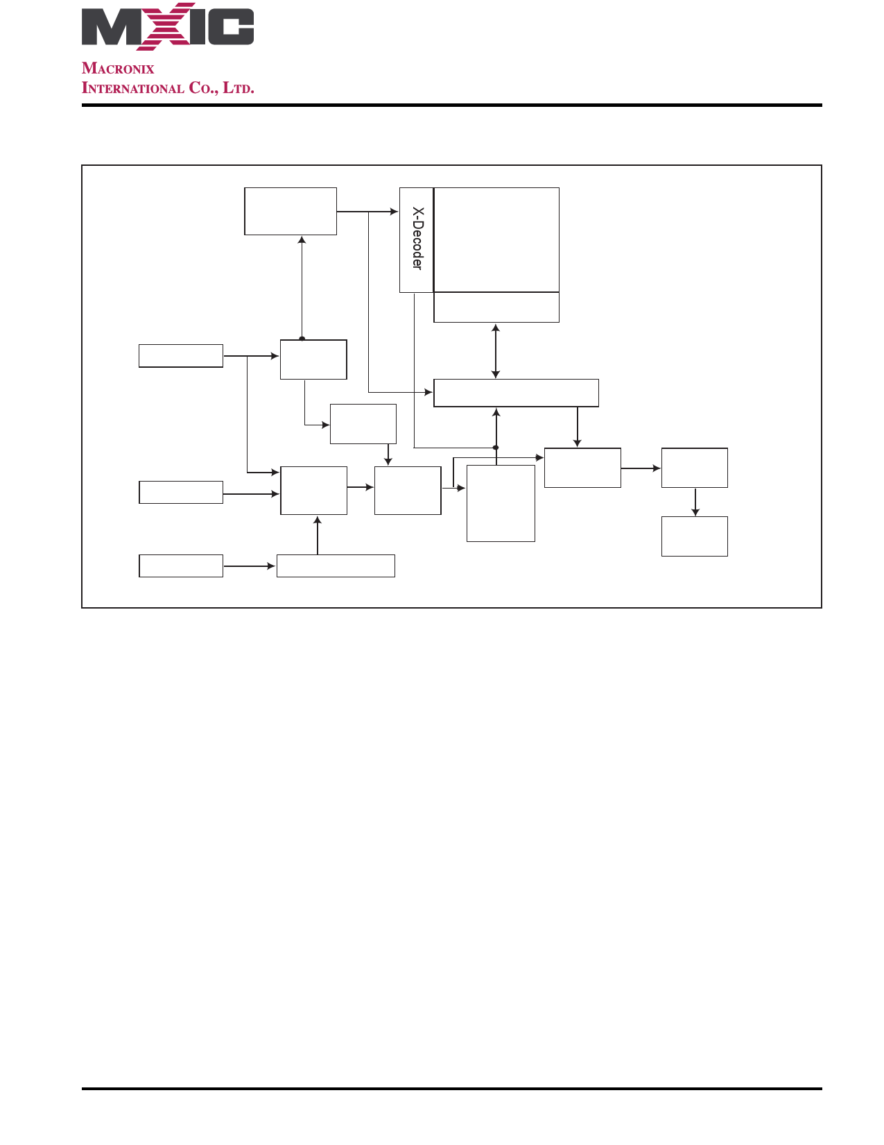
BLOCK DIAGRAM
Address
Generator
MX25L512C
Memory Array
SI
CS#
SCLK
Page Buffer
Data
Register
SRAM
Buffer
Mode
Logic
State
Machine
Y-Decoder
HV
Generator
Sense
Amplifier
Clock Generator
Output
Buffer
SO
P/N: PM1469
REV. 1.2, OCT. 06, 2009
5
5 Page 
MX25L512C
(4) Read Status Register (RDSR)
The RDSR instruction is for reading Status Register Bits. The Read Status Register can be read at any time (even in
program/erase/write status register condition) and continuously. It is recommended to check the Write in Progress (WIP)
bit before sending a new instruction when a program, erase, or write status register operation is in progress.
The sequence of issuing RDSR instruction is: CS# goes low→sending RDSR instruction code→Status Register
data out on SO (see Figure. 14)
The definition of the status register bits is as below:
WIP bit. The Write in Progress (WIP) bit, a volatile bit, indicates whether the device is busy in program/erase/write
status register progress. When WIP bit sets to 1, which means the device is busy in program/erase/write status
register progress. When WIP bit sets to 0, which means the device is not in progress of program/erase/write status
register cycle.
WEL bit. The Write Enable Latch (WEL) bit, a volatile bit, indicates whether the device is set to internal write enable
latch. When WEL bit sets to 1, which means the internal write enable latch is set, the device can accept program/
erase/write status register instruction. When WEL bit sets to 0, which means no internal write enable latch; the de-
vice will not accept program/erase/write status register instruction.
BP1, BP0 bits. The Block Protect (BP1, BP0) bits, non-volatile bits, indicate the protected area(as defined in table
1) of the device to against the program/erase instruction without hardware protection mode being set. To write the
Block Protect (BP1, BP0) bits requires the Write Status Register (WRSR) instruction to be executed. Those bits
define the protected area of the memory to against Page Program (PP), Sector Erase (SE), Block Erase (BE) and
Chip Erase(CE) instructions (only if all Block Protect bits set to 0, the CE instruction can be executed)
SRWD bit. The Status Register Write Disable (SRWD) bit, non-volatile bit, is operated together with Write Protec-
tion (WP#) pin for providing hardware protection mode. The hardware protection mode requires SRWD sets to 1
and WP# pin signal is low stage. In the hardware protection mode, the Write Status Register (WRSR) instruction is
no longer accepted for execution and the SRWD bit and Block Protect bits (BP1, BP0) are read only.
bit7 bit6 bit5 bit4 bit3 bit2 bit1 bit0
SRWD (status
register write
protect)
0
0
0
BP1
(level of
protected
block)
BP0
(level of
protected
block)
WEL
WIP
(write enable (write in
latch) progress bit)
1=status
register write
disable
(note 1)
(note 1)
1=write
enable
0=not write
enable
1=write
operation
0=not in write
operation
Note: 1. See the table "Protected Area Sizes".
2. The endurance cycles of protect bits are 100,000 cycles; however, the tW time out spec of protect bits is
relaxed as tW = N x 15ms (N is a multiple of 10,000 cycles, ex. N = 2 for 20,000 cycles) after 10,000 cycles
on those bits.
P/N: PM1469
REV. 1.2, OCT. 06, 2009
11
11 Page | ||
| Páginas | Total 30 Páginas | |
| PDF Descargar | [ Datasheet MX25L512C.PDF ] | |
Hoja de datos destacado
| Número de pieza | Descripción | Fabricantes |
| MX25L512 | 512K-BIT [x 1] CMOS SERIAL FLASH | Macronix International |
| MX25L5121E | 512K-BIT [x 1] CMOS SERIAL FLASH Memory | Macronix International |
| MX25L51245G | FLASH MEMORY | MACRONIX |
| MX25L512C | 512K-BIT [x 1] CMOS SERIAL FLASH | Macronix International |
| Número de pieza | Descripción | Fabricantes |
| SLA6805M | High Voltage 3 phase Motor Driver IC. |
Sanken |
| SDC1742 | 12- and 14-Bit Hybrid Synchro / Resolver-to-Digital Converters. |
Analog Devices |
|
DataSheet.es es una pagina web que funciona como un repositorio de manuales o hoja de datos de muchos de los productos más populares, |
| DataSheet.es | 2020 | Privacy Policy | Contacto | Buscar |
