|
|
|
PDF AS5SS512K36D Data sheet ( Hoja de datos )
| Número de pieza | AS5SS512K36D | |
| Descripción | 512K x 36 SSRAM | |
| Fabricantes | Micross Components | |
| Logotipo | ||
Hay una vista previa y un enlace de descarga de AS5SS512K36D (archivo pdf) en la parte inferior de esta página. Total 15 Páginas | ||
|
No Preview Available !
SSRAM
AS5SS512K36
512K x 36 SSRAM
Flow-Through SRAM
No Bus Latency
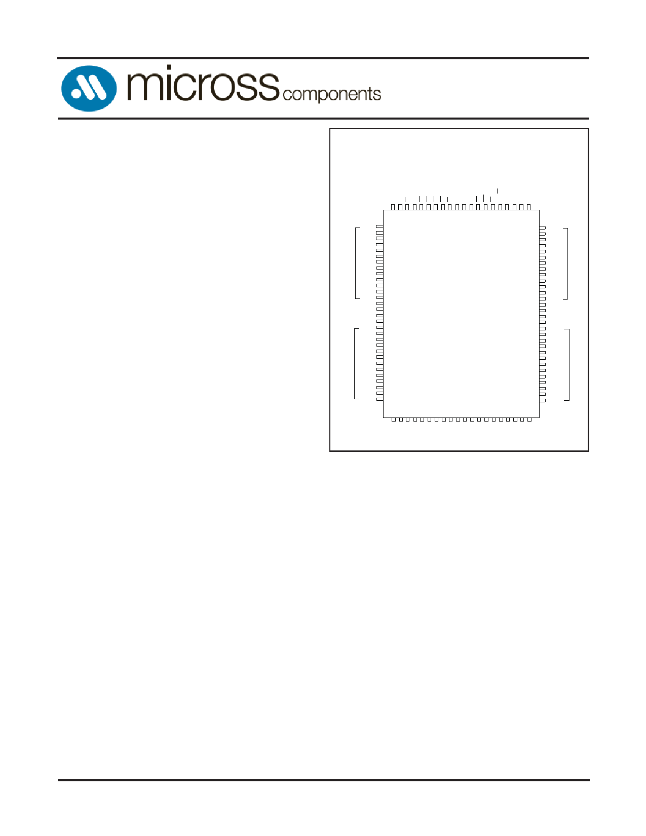
PIN ASSIGNMENT
(Top View)
100-Pin TQFP (DQ)
AVAILABLE AS MILITARY
SPECIFICATIONS
•MIL-STD-883
FEATURES
• Pin compatible and functionally equivalent to ZBT devices.
• Supports 133MHz bus operations with zero wait states
-Data is transferred on every clock
• Internally self-timed output buffer control to eliminate the need
to use asynchronous OE\
• Registered inputs for Flow-Through operation
• Byte Write capability
• Common I/O architecture
• Fast clock-to-output times
-6.5ns (for 133 MHz device)*
-8.5ns (for 100 MHz device)
• Single 3.3V -5% and +1-% power supply V
DD
• Separate VDD for 3.3V or 2.5V I/O
• Clock Enable (CEN\) pin to suspend operation
• Synchronous self-timed writes
• Available in 100-pin TSOP package.**
• Burst Capability - linear or interleaved burst order
• No bus latency architecture eliminated dead cycles between write
and read cyccles
OPTIONS
• Timing
6.5ns access
8.5ns access
MARKING
-6.5*
-8.5
• Operating Temperature Ranges
Military (-55oC to +125oC) XT
Industrial (-40oC to +85oC) IT
• Package(s)**
100-pin TQFP
DQ
NOTES:
* 6.5ns speed available with IT option only.
**Contact factory for BGA package interests.
GENERAL DESCRIPTION
The AS5SS512K36D is is a 3.3V, 512K x 36 Synchronous
flow through Burst SRAM designed specifically to support
unlimited true back-to-back Read/Write operations with no
wait state insertion. The AS5SS512K36D is equipped with the
advanced No Bus Latency logic required to enable consecutive
Read/Write operations with data being transferred on every
clock cycle. This feature dramatically improves the throughput
BYTE C
BYTE D
DQPC
DQC
DQC
VDDQ
VSS
DQC
DQC
DQC
DQC
VSS
VDDQ
DQC
DQC
NC
VDD
NC
VSS
DQD
DQD
VDDQ
VSS
DQD
DQD
DQD
DQD
VSS
VDDQ
DQD
DQD
DQPD
1
2
3
4
5
6
7
8
9
10
11
12
13
14
15
16
17
18
19
20
21
22
23
24
25
26
27
28
29
30
CY7C1371D
80 DQPB
79 DQB
78 DQB
77 VDDQ
76 VSS
75
74
DQB
DQB
BYTE B
73 DQB
72 DQB
71 VSS
70 VDDQ
69 DQB
68 DQB
67 VSS
66 NC
65 VDD
64 ZZ
63 DQA
62 DQA
61 VDDQ
60 VSS
59 DQA
58 DQA
57
DQA
BYTE A
56 DQA
55 VSS
54 VDDQ
53 DQA
52 DQA
51 DQPA
All synchronous inputs pass through input registers controlled by the
rising edge of the clock. The clock input is qualified by the Clock
Enable (CEN) signal, which when deasserted suspends operation and
extends the previous clock cycle. Maximum access delay from the
clock rise is 6.5 ns (133-MHz device). Write operations are controlled
by the two or four Byte Write Select (BWX) and a Write Enable (WE)
input. All writes are conducted with on-chip synchronous self-timed
write circuitry. Three synchronous Chip Enables (CE1, CE2, CE3)
and an asynchronous Output Enable (OE) provide for easy bank
selection and output tri-state control. To avoid bus contention, the
output drivers are synchronously tri-stated during the data portion of
a write sequence.
All synchronous inputs pass through input registers controlled by
the rising edge of the clock. The clock input is qualified by the Clock
Enable (CEN\) signal, which when deasserted suspends operation and
extends the previous clock cycle.
Write operations are controlled by the Byte Write Selects (BWS\
a,b,c,d) and a Write Enable (WE\) input. All writes are conducted
with on-chip synchronous self-timed write circuitry.
Synchronous Chip Enable (CE1\, CE2, CE3\) and an
asynchronous Output Enable (OE\) provide for easy bank selection
and output three-state control. In order to avoid bus contention, the
output drivers are synchronously three-stated during the data portion
of a write sequence.
For more products and information
of data through the SRAM, especially in systems that require
frequent Write-Read transitions.
please visit our web site at
www.micross.com
AS5SS512K36
Rev. 0.6 01/10
Micross Components reserves the right to change products or specifications without notice.
1
1 page 
SSRAM
AS5SS512K36
CYCLE DESCRIPTION TRUTH TABLE2,3,4,5,6,7,8
OPERATION
Deselect Cycle
Deselect Cycle
Deselect Cycle
Continue Deselect Cycle
Read Cycle (Begin Burst)
Read Cycle (Continue Burst)
NOP/ Dummy Read (Continue Burst)
Dummy Read (Continue Burst)
Write Cycle (Begin Burst)
Write Cycle (Continue Burst)
NOP/Write Abort (Continue Burst)
Write Abort (Continue Burst)
Ignore Clock Edge (Stall)
Sleep Mode
ADDRESS CE1\ CE2 CE3\
None
HXX
None
XXH
None X L X
None
XXX
External L H L
Next
XXX
External L H L
Next
XXX
External L H L
Next
XXX
None L H L
Next
XXX
Current X X X
None
XXX
ZZ ADV/LD\ WE\ BW\x OE\ CEN\
L L XXXL
L L XXXL
L L XXXL
L H XXXL
L L HXL L
L H XXL L
L L HXHL
L H XXHL
L L LLXL
L H XLXL
L L LHXL
L H XHXL
L X XXXH
H X XXXX
CLK
L->H
L->H
L->H
L->H
L->H
L->H
L->H
L->H
L->H
L->H
L->H
L->H
L->H
X
DQ
Tri-State
Tri-State
Tri-State
Tri-State
Data Out (Q)
Data Out (Q)
Tri-State
Tri-State
Data In (Q)
Data In (Q)
Tri-State
Tri-State
-
Tri-State
INTERLEAVED BURST SEQUENCE2,3,9
FIRST
ADDRESS
A[1:0]
00
01
10
11
SECOND
ADDRESS
A[1:0]
01
00
11
10
THIRD
ADDRESS
A[1:0]
10
11
00
01
FOURTH
ADDRESS
A[1:0]
11
10
01
00
LINEAR BURST SEQUENCE2,3,9
FIRST
ADDRESS
A[1:0]
00
01
10
11
SECOND
ADDRESS
A[1:0]
01
10
11
00
THIRD
ADDRESS
A[1:0]
10
11
00
01
FOURTH
ADDRESS
A[1:0]
11
00
01
10
NOTES:
2. X = “Don’t Care.” H = Logic HIGH, L = Logic LOW. BWX = 0 signifies at least one Byte Write Select is active, BWX = Valid signifies that the desired byte write
selects are asserted, see truth table for details.
3. Write is defined by BWX, and WE. See truth table for Read/Write.
4. When a write cycle is detected, all IOs are tri-stated, even during byte writes.
5. The DQs and DQPX pins are controlled by the current cycle and the OE signal. OE is asynchronous and is not sampled with the clock.
6. CEN = H, inserts wait states.
7. Device powers up deselected and the IOs in a tri-state condition, regardless of OE.
8. OE is asynchronous and is not sampled with the clock rise. It is masked internally during write cycles. During a read cycle DQs and DQPX = Tri-state when OE
is inactive or when the device is deselected, and DQs and DQPX = data when OE is active.
9. Table only lists a partial listing of the byte write combinations. Any Combination of BWX is valid Appropriate write is based on which byte write is active.
AS5SS512K36
Rev. 0.6 01/10
Micross Components reserves the right to change products or specifications without notice.
5
5 Page 
SSRAM
AS5SS512K36
SWITCHING WAVEFORMS: NOP, STALL & DESELECT CYCLES25, 26, 28
CLK
CEN
CE
ADV/LD
WE
BW [A:D]
ADDRESS
1
A1
2
A2
DQ D(A1)
COMMAND WRITE
READ
D(A1) Q(A2)
34
A3
Q(A2)
STALL READ
Q(A3)
56
A4
Q(A3)
WRITE STALL
D(A4)
7 8 9 10
D(A4)
NOP
A5
tCHZ
Q(A5)
tDOH
READ DESELECT CONTINUE
Q(A5) DESELECT
DON’T CARE
UNDEFINED
Note:
28. The IGNORE CLOCK EDGE or STALL cycle (Clock 3) illustrates CEN being used to create a pause. A write is not performed during this cycle.
AS5SS512K36
Rev. 0.6 01/10
11
Micross Components reserves the right to change products or specifications without notice.
11 Page | ||
| Páginas | Total 15 Páginas | |
| PDF Descargar | [ Datasheet AS5SS512K36D.PDF ] | |
Hoja de datos destacado
| Número de pieza | Descripción | Fabricantes |
| AS5SS512K36 | 512K x 36 SSRAM | Micross Components |
| AS5SS512K36D | 512K x 36 SSRAM | Micross Components |
| AS5SS512K36D | 512K x 36 SSRAM | Micross Components |
| Número de pieza | Descripción | Fabricantes |
| SLA6805M | High Voltage 3 phase Motor Driver IC. |
Sanken |
| SDC1742 | 12- and 14-Bit Hybrid Synchro / Resolver-to-Digital Converters. |
Analog Devices |
|
DataSheet.es es una pagina web que funciona como un repositorio de manuales o hoja de datos de muchos de los productos más populares, |
| DataSheet.es | 2020 | Privacy Policy | Contacto | Buscar |