|
|
|
PDF MT48H4M16LF Data sheet ( Hoja de datos )
| Número de pieza | MT48H4M16LF | |
| Descripción | Mobile SDRAM | |
| Fabricantes | Micron Technology | |
| Logotipo | ||
Hay una vista previa y un enlace de descarga de MT48H4M16LF (archivo pdf) en la parte inferior de esta página. Total 30 Páginas | ||
|
No Preview Available !
Mobile SDRAM
MT48H4M16LF – 1 Meg x 16 x 4 banks
64Mb: 4 Meg x 16 Mobile SDRAM
Features
Features
• 1.70–1.95V
• Fully synchronous; all signals registered on positive
edge of system clock
• Internal pipelined operation; column address can be
changed every clock cycle
• Internal banks for hiding row access/precharge
• Programmable burst lengths: 1, 2, 4, 8, or continuous
page1
• Auto precharge, includes concurrent auto precharge
• Self refresh mode
• 64ms, 4,096-cycle refresh
• LVTTL-compatible inputs and outputs
• Partial-array self refresh (PASR) power-saving mode
• On-die temperature-compensated self refresh
(TCSR)
• Deep power-down (DPD) mode
• Programmable output drive strength
• Operating temperature ranges
– Commercial (0°C to +70°C)
– Industrial (–40°C to +85°C)
Notes: 1. For continuous page burst, contact factory
for availability.
Options
• VDD/VDDQ
– 1.8V/1.8V
• Configurations
– 4 Meg x 16 (1 Meg x 16 x 4 banks)
• Plastic “green” package
– 54-ball VFBGA, 8mm x 8mm
• Timing (cycle time)
– 7.5ns @ CL = 3 (133 MHz)
– 8ns @ CL = 3 (125 MHz)
• Operating temperature
– Commercial (0°C to +70°C)
– Industrial (–40°C to +85°C)
• Die revision designator
Marking
H
4M16
B4
-75
-8
None
IT
:H
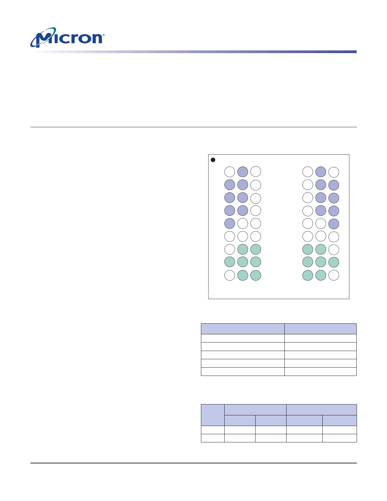
Figure 1: 54-Ball VFBGA Ball Assignment
(Top View)
123456789
A VSS DQ15 VSSQ
VDDQ DQ0
VDD
B DQ14 DQ13 VDDQ
VSSQ
DQ2
DQ1
C DQ12 DQ11 VSSQ
VDDQ DQ4
DQ3
D DQ10 DQ9 VDDQ
VSSQ
DQ6
DQ5
E
DQ8
NC
VSS
VDD LDQM DQ7
F UDQM CLK CKE
CAS# RAS#
WE#
G NC A11 A9
BA0 BA1
CS#
H A8 A7 A6
A0 A1 A10
J VSS A5 A4
Top view
(Ball down)
A3 A2 VDD
Table 1: Address Table
Configuration
Refresh count
Row addressing
Bank addressing
Column addressing
4 Meg x 16
1 Meg x 16 x 4 banks
4K
4K (A0–A11)
4 (BA0, BA1)
256 (A0–A7)
Table 2:
Key Timing Parameters
CL = CAS (READ) latency
Speed
Grade
-75
-8
Clock Rate (MHz)
CL = 2
104
83
CL = 3
133
125
Access Time
CL = 2
8ns
8ns
CL = 3
6ns
6ns
PDF: 09005aef8237ed98/Source: 09005aef8237ed68
64mb_x16_Mobile SDRAM_Y24L_1.fm - Rev. C 10/07 EN
1 Micron Technology, Inc., reserves the right to change products or specifications without notice.
©2006 Micron Technology, Inc. All rights reserved.
Products and specifications discussed herein are subject to change by Micron without notice.
1 page 
64Mb: 4 Meg x 16 Mobile SDRAM
General Description
Figure 2: Part Numbering Diagram
Example Part Number: MT48H4M16LFB4-8 IT :H
MT48 VDD/ Configuration
VDDQ
–
Package
Speed
Temp Revision
VDD/VDDQ
1.8V/1.8V
H
Configuration
4 Meg x16 4M16LF
Package
54-ball VFBGA (8mm x 8mm) ”green”
B4
:H Design revision
Operating Temp.
None Commercial
IT Industrial
Speed Grade
-75 7.5ns
-8 8ns
General Description
The Micron® 64Mb SDRAM is a high-speed CMOS, dynamic random access memory
containing 67,108,864 bits. It is internally configured as a quad-bank DRAM with a
synchronous interface (all signals are registered on the positive edge of the clock signal,
CLK). Each of the x16’s 16,777,216-bit banks is organized as 4,096 rows by 256 columns
by 16 bits.
Read and write accesses to the SDRAM are burst oriented; accesses start at a selected
location and continue for a programmed number of locations in a programmed
sequence. Accesses begin with the registration of an ACTIVE command, which is then
followed by a READ or WRITE command. The address bits registered coincident with the
ACTIVE command are used to select the bank and row to be accessed (BA0, BA1 select
the bank; A0–A11 select the row). The address bits registered coincident with the READ
or WRITE command are used to select the starting column location for the burst access.
The SDRAM provides for programmable read or write burst lengths of 1, 2, 4, or 8 loca-
tions with a burst terminate option. An auto precharge function may be enabled to
provide a self-timed row precharge that is initiated at the end of the burst sequence.
The 64Mb SDRAM uses an internal pipelined architecture to achieve high-speed opera-
tion. This architecture is compatible with the 2n rule of prefetch architectures, but it also
enables the column address to be changed on every clock cycle to achieve a high-speed,
fully random access. Precharging one bank while accessing one of the other three banks
will hide the PRECHARGE cycles and provide seamless high-speed, random-access
operation.
The 64Mb SDRAM is designed to operate in 1.8V, low-power memory systems. An auto
refresh mode is provided, along with a power-saving, deep power-down mode. All inputs
and outputs are LVTTL-compatible.
PDF: 09005aef8237ed98/Source: 09005aef8237ed68
64mb_x16_Mobile SDRAM_Y24L_2.fm - Rev. C 10/07 EN
5 Micron Technology, Inc., reserves the right to change products or specifications without notice.
©2006 Micron Technology, Inc. All rights reserved.
5 Page 
Figure 5: CAS Latency
CLK
Command
DQ
T0 T1
READ
NOP
tLZ
tAC
CL = 2
64Mb: 4 Meg x 16 Mobile SDRAM
Mode Register Definition
T2 T3
NOP
tOH
DOUT
CLK
Command
T0
READ
DQ
T1 T2
NOP
CL = 3
NOP
tLZ
tAC
T3 T4
NOP
tOH
DOUT
Don’t Care
Undefined
Operating Mode
The normal operating mode is selected by setting M7 and M8 to zero; the other combi-
nations of values for M7 and M8 are reserved for future use. The programmed burst
length applies to both read and write bursts.
Reserved states must not be used; unknown operation or incompatibility with future
versions may result.
Write Burst Mode
When M9 = 0, the burst length programmed via M0–M2 applies to both READ and
WRITE bursts; when M9 = 1, the programmed burst length applies to READ bursts, but
write accesses are single-location accesses.
Extended Mode Register
The extended mode register controls the functions beyond those controlled by the mode
register. These additional functions are special features of the mobile device. They
include temperature-compensated self refresh (TCSR) control, partial-array self refresh
(PASR), and output drive strength.
The extended mode register is programmed via the MODE REGISTER SET command
with BA = 1 and BA = 0 and retains the stored information until it is programmed again
or the device loses power.
The extended mode register must be loaded when all banks are idle and no bursts are in
progress, and the controller must wait tMRD before initiating any subsequent operation.
Violating any of these requirements will result in unspecified operation.
PDF: 09005aef8237ed98/Source: 09005aef8237ed68
64mb_x16_Mobile SDRAM_Y24L_2.fm - Rev. C 10/07 EN
11
Micron Technology, Inc., reserves the right to change products or specifications without notice.
©2006 Micron Technology, Inc. All rights reserved.
11 Page | ||
| Páginas | Total 30 Páginas | |
| PDF Descargar | [ Datasheet MT48H4M16LF.PDF ] | |
Hoja de datos destacado
| Número de pieza | Descripción | Fabricantes |
| MT48H4M16LF | Mobile SDRAM | Micron Technology |
| Número de pieza | Descripción | Fabricantes |
| SLA6805M | High Voltage 3 phase Motor Driver IC. |
Sanken |
| SDC1742 | 12- and 14-Bit Hybrid Synchro / Resolver-to-Digital Converters. |
Analog Devices |
|
DataSheet.es es una pagina web que funciona como un repositorio de manuales o hoja de datos de muchos de los productos más populares, |
| DataSheet.es | 2020 | Privacy Policy | Contacto | Buscar |