|
|
|
PDF RS2112 Data sheet ( Hoja de datos )
| Número de pieza | RS2112 | |
| Descripción | Primary-Side Regulation PWM Power Switch | |
| Fabricantes | Orister | |
| Logotipo | ||
Hay una vista previa y un enlace de descarga de RS2112 (archivo pdf) en la parte inferior de esta página. Total 9 Páginas | ||
|
No Preview Available !
RS2111/RS2112
Primary-Side Regulation PWM Power Switch
Description
RS2111/RS2112 is an offline PWM Power switch for low power AC/DC charger and adaptor
applications. It operates in primary-side sensing and regulation. Consequently, opto-coupler
and TL431 could be eliminated from design. Proprietary Constant Voltage (CV) and Constant
Current (CC) control is integrated as shown in the figure below.
V0
Page No. : 1/9
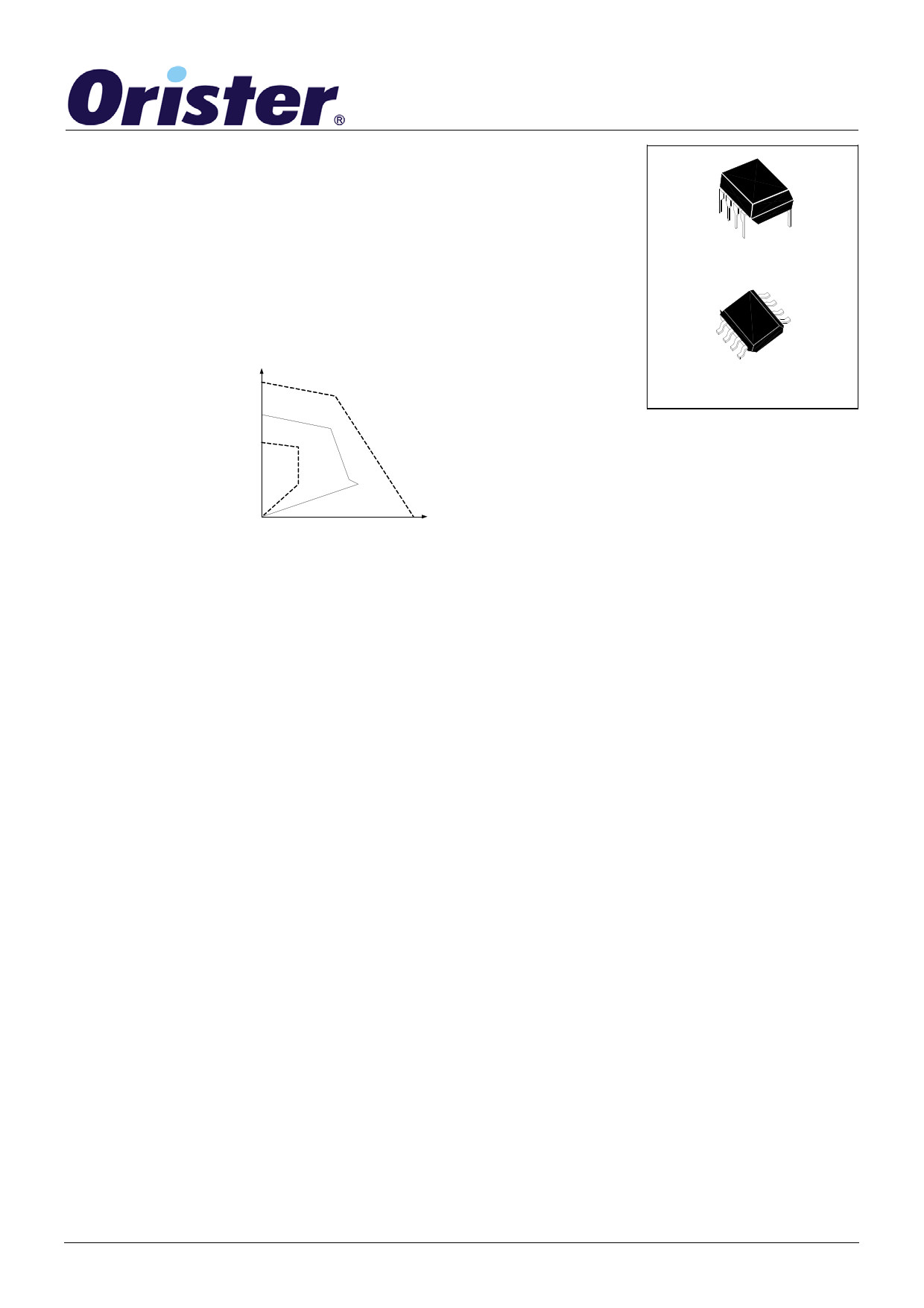
8-Lead Plastic DIP-8
Package Code: P
8-Lead Plastic SOP-8
Package Code: S
I0
Fig1. Typical CC/CV Curve
In CC control, the current and output power setting can be adjusted externally by the sense resistor Rs at CS pin. In CV control,
multi-mode operations are utilized to achieve high performance and high efficiency. Device operates in fixed frequency mode at
large load conditions, frequency reduction mode at light/medium load and ‘Extended burst mode’ at No/light load conditions.
RS2111/RS2112 offers power on soft start control and complete protection coverage with auto-recovery features including
Cycle-by-Cycle current limiting, VDD over-voltage clamp and UVLO, fail-safe protection for open loop fault condition. Excellent
EMI performance is achieved with Orister proprietary frequency Jiggling technique together with soft switching control at the totem
pole gate drive output with No-Y Cap design.
Features
Primary-side Sensing and Regulation With No 431 and Opto-coupler
Multi-mode operation for High Efficiency
Programmable CV and CC Regulation
Adjustable Constant Current and Output Power setting
Frequency Jiggling and Adjustable Gate Drive Greatly Improved EMI
Power on Soft-start Time (4ms)
Burst mode Control for Improved Efficiency and Minimum standby Design
Built-in Leading Edge Blanking (LEB)
Cycle-by-Cycle Current Limiting
VDD Under Voltage Lockout with Hysteresis (UVLO)
VDD Over Voltage Shutdown and Clamp
Auto-restart in Over Voltage condition
Fail-safe protection for open loop fault condition
Compatible with OB2211/OB2212
Pb-Free SOP-8L & DIP-8L
Applications
Low Power AC/DC offline SMPS
Cell Phone Charge
Digital Cameras Charger
Small Power Adaptor
Auxiliary Power for PC, TV etc.
Linear Regulator/RCC Replacement
DS-RS2111/RS2112-01 Oct, 2008
www.Orister.com
1 page 
Page No. : 5/9
Operation switching frequency
The switching frequency of RS2111/RS2112 is internally set and adjusted according to CC/CV operation. No external frequency
setting components are required.
Frequency Jiggling for EMI improvement
The frequency Jiggling/jittering (switching frequency modulation is implemented in MCD6211. The oscillation frequency is
modulated with a pseudo random source so that the tone energy is spread out. The spread spectrum minimizes the conduction
band EMI and therefore eases the system design.
Current sensing and Leading Edge Blanking
Cycle-by-Cycle current limiting is offered in RS2111/RS2112 current mode PWM control. The switch current is detected by a sense
resistor into the CS pin. An internal leading edge blanking circuit chops off the sensed voltage spike at initial internal power
MOSFET on state due to snubber diode reverse recovery and surge current of power MOSFET due to Drain/source Cap so that
the external RC filtering on sense input is no longer needed. The PWM duty cycle is determined by the current sense input voltage
and the EA output voltage.
Adjustable Driver Capability
The internal power MOSFET in RS2111/RS2112 is driven by a dedicated gate driver for power switch control. Too weak the gate
drive strength results in higher conduction and switch loss of MOSFET while too strong gate drive compromises EMI.
A good tradeoff is achieved through the built-in totem pole gate design with right output strength control. The gate drive strength
can be adjusted externally by a resistor connected between VDD and VDDG. The low idle loss and good EMI system design is
possible with this dedicated control scheme.
Protection Control
Good power supply system reliability is achieved with its rich protection features including Cycle-by-Cycle current limiting (OCP),
VDD over voltage protection and clamp, Power on Soft Start, and Under Voltage Lockout on VDD (UVLO).
VDD is supplied by transformer auxiliary winding output. PWM output of RS2111/RS2112 is shut down when VDD is higher than
30V due to over voltage protection triggering. The output of RS2111/RS2112 is shut down when VDD drops below UVLO(ON) limit
and Switcher enters power on start-up sequence thereafter.
DS-RS2111/RS2112-01 Oct, 2008
www.Orister.com
5 Page | ||
| Páginas | Total 9 Páginas | |
| PDF Descargar | [ Datasheet RS2112.PDF ] | |
Hoja de datos destacado
| Número de pieza | Descripción | Fabricantes |
| RS2111 | Primary-Side Regulation PWM Power Switch | Orister |
| RS2112 | Primary-Side Regulation PWM Power Switch | Orister |
| RS2112 | High Precision CC/CV Primary-Side PWM Power Switch | PTC |
| Número de pieza | Descripción | Fabricantes |
| SLA6805M | High Voltage 3 phase Motor Driver IC. |
Sanken |
| SDC1742 | 12- and 14-Bit Hybrid Synchro / Resolver-to-Digital Converters. |
Analog Devices |
|
DataSheet.es es una pagina web que funciona como un repositorio de manuales o hoja de datos de muchos de los productos más populares, |
| DataSheet.es | 2020 | Privacy Policy | Contacto | Buscar |