|
|
|
PDF NCT218 Data sheet ( Hoja de datos )
| Número de pieza | NCT218 | |
| Descripción | High Accuracy Temperature Monitor | |
| Fabricantes | ON Semiconductor | |
| Logotipo | ||
Hay una vista previa y un enlace de descarga de NCT218 (archivo pdf) en la parte inferior de esta página. Total 18 Páginas | ||
|
No Preview Available !
NCT218
Low Voltage, High
Accuracy Temperature
Monitor with I2C Interface
The NCT218 is a dual−channel digital thermometer and
undertemperature/overtemperature alarm, intended for use in thermal
management systems requiring low power and size. The NCT218
operates over a supply range of 1.4 V to 2.75 V making it possible to
use it in a wide range of applications including low power devices.
The NCT218 can measure the temperature of a remote thermal diode
accurate to ±1°C and the ambient temperature accurate to ±1.75°C.
The device operates over a wide temperature range of −40°C to
+125°C.
The NCT218 includes series resistance cancellation, where up to
500 W (typical) of resistance in series with the temperature monitoring
diode can be automatically cancelled from the temperature result,
allowing noise filtering. The NCT218 has a configurable ALERT
output and overtemperature shutdown THERM pin.
Communication with the NCT218 is accomplished via the I2C
interface which is compatible with industry standard protocols.
Through this interface the NCT218s internal registers may be
accessed. These registers allow the user to read the current
temperature from both the local (ambient) and remote channels,
change the configuration settings and adjust each channels limits.
An ALERT output signals when the on−chip or remote temperatures
are out of range. The THERM output is a comparator output that can
be used to shut down the system if it exceeds the programmed limit.
The ALERT output can be reconfigured as a second THERM output, if
required.
Features
• Small DFN Package
• On−Chip and Remote Temperature Sensor
• Low Voltage Operation: 1.4 V to 2.75 V
• Low Quiescent Current:
♦ 44 mA Normal Mode (max)
♦ 20 mA Shutdown (max)
• Power Saving Shutdown Mode
• Operating Temperature Range of −40°C to 125°C
• Series Resistance Cancellation up to 500 W
• Low D− bias for Operation with Low Voltage Processors
• 2−wire I2C Serial Interface
• Programmable Over/Undertemperature Limits
• These are Pb−Free Devices
Applications
• Smart Phones, Tablet PCs, Satellite Navigation, Smart Batteries
© Semiconductor Components Industries, LLC, 2013
December, 2013 − Rev. 2
1
http://onsemi.com
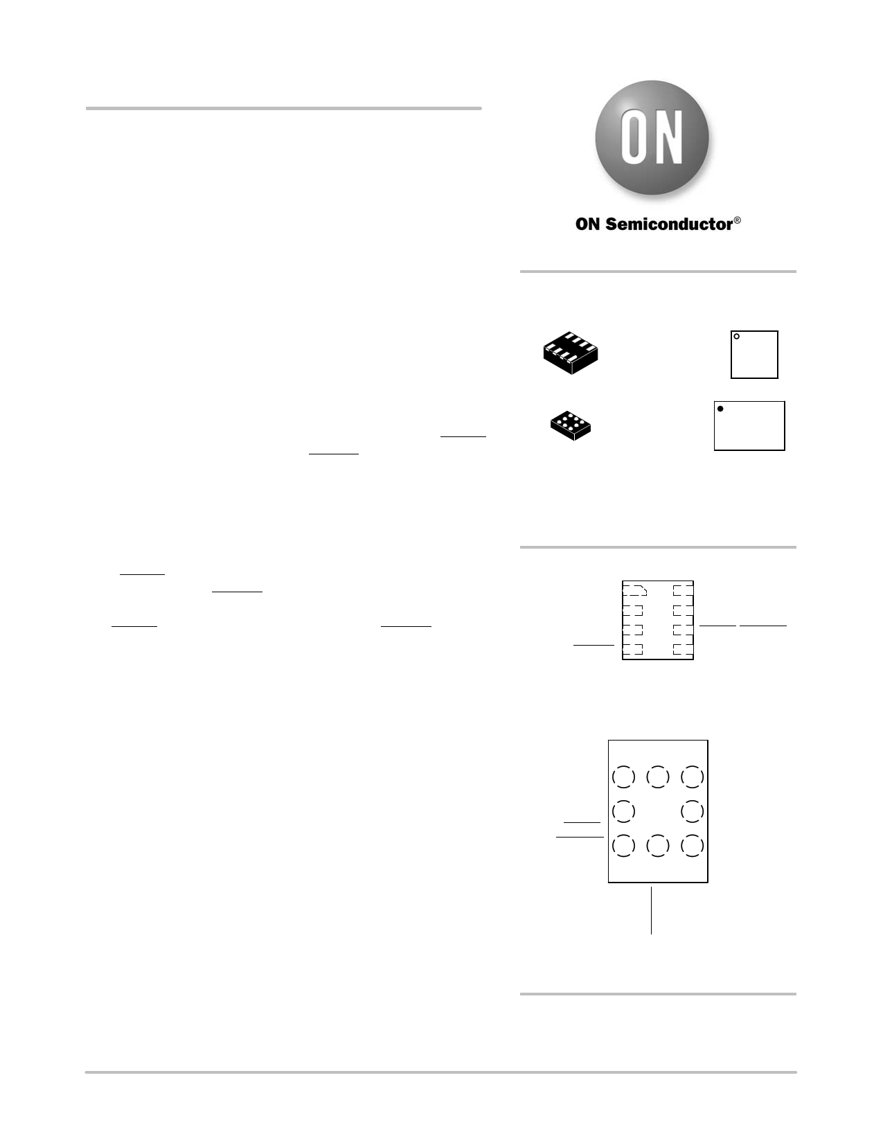
MARKING
DIAGRAMS
DFN8
MT SUFFIX
CASE 511BU
1
T2 MG
G
WLCSP8
CASE 567DH
NCT218
AYWW
M = Date Code
AY = Assembly year
WW = Work Week
G = Pb−Free Device
(Note: Microdot may be in either location)
PIN ASSIGNMENTS
VDD
D+
D−
THERM
18
27
36
45
DFN8
(Top View)
SCL
SDA
ALERT/THERM2
GND
SDA C1 B1 A1 VDD
GND C2
A2 D+
ALERT/
THERM2 C3 B3 A3 D−
WLCSP8
(Top View)
ORDERING INFORMATION
See detailed ordering and shipping information on page 16 of
this data sheet.
Publication Order Number:
NCT218/D
1 page 
NCT218
Theory of Operation
The NCT218 is a local and remote temperature sensor and
over/under temperature alarm, with the added ability to
automatically cancel the effect of 500 W (typical) of
resistance in series with the temperature monitoring diode.
When the NCT218 is operating normally, the on−board
ADC operates in a free running mode. The analog input
multiplexer alternately selects either the on−chip
temperature sensor to measure its local temperature or the
remote temperature sensor. The ADC digitizes these signals
and the results are stored in the local and remote temperature
value registers.
The local and remote measurement results are compared
with the corresponding high, low, and THERM temperature
limits, stored in eight on−chip registers. Out−of−limit
comparisons generate flags that are stored in the status
register. A result that exceeds the high temperature limit or
the low temperature limit causes the ALERT output to
assert. The ALERT output also asserts if an external diode
fault is detected. Exceeding the THERM temperature limits
causes the THERM output to assert low. The ALERT output
can be reprogrammed as a second THERM output.
The limit registers are programmed and the device
controlled and configured via the serial I2C. The contents of
any register are also read back via the I2C. Control and
configuration functions consist of switching the device
between normal operation and standby mode, selecting the
temperature measurement range, masking or enabling the
ALERT output, switching Pin 6 between ALERT and
THERM2, and selecting the conversion rate.
Series Resistance Cancellation
Parasitic resistance to the D+ and D− inputs to the
NCT218, seen in series with the remote diode, is caused by
a variety of factors, including PCB track resistance and track
length. This series resistance appears as a temperature ofset
in the remote sensor’s temperature measurement. This error
typically causes a 0.5°C offset per ohm of parasitic
resistance in series with the remote diode.
The NCT218 automatically cancels the effect of this
series resistance on the temperature reading, giving a more
accurate result, without the need for user characterization of
this resistance. The NCT218 is designed to automatically
cancel typically up to 150 W of resistance. By using an
advanced temperature measurement method, this process is
transparent to the user. This feature permits resistances to be
added to the sensor path to produce a filter, allowing the part
to be used in noisy environments. See the section on Noise
Filtering for more details.
Temperature Measurement Method
A simple method of measuring temperature is to exploit
the negative temperature coefficient of a diode, measuring
the base emitter voltage (VBE) of a transistor operated at
constant current. However, this technique requires
calibration to null the effect of the absolute value of VBE,
which varies from device to device.
The technique used in the NCT218 measures the change
in VBE when the device operates at three different currents.
Previous devices used only two operating currents, but it is
the use of a third current that allows automatic cancellation
of resistances in series with the external temperature sensor.
Figure 4 shows the input signal conditioning used to
measure the output of an external temperature sensor. This
figure shows the external sensor as a substrate transistor, but
it can equally be a discrete transistor. If a discrete transistor
is used, the collector is not grounded but is linked to the base.
To prevent ground noise interfering with the measurement,
the more negative terminal of the sensor is not referenced to
ground, but is biased above ground by an internal resistor at
the D− input. C1 may be added as a noise filter (a
recommended maximum value of 1000 pF). However, a
better option in noisy environments is to add a filter, as
described in the Noise Filtering section. See the Layout
Considerations section for more information on C1.
To measure DVBE, the operating current through the
sensor is switched among three related currents. As shown
in Figure 4, N1 x I and N2 x I are different multiples of the
current, I. The currents through the temperature diode are
switched between I and N1 x I, giving DVBE1; and then
between I and N2 x I, giving DVBE2. The temperature is then
calculated using the two DVBE measurements. This method
also cancels the effect of any series resistance on the
temperature measurement.
The resulting DVBE waveforms are passed through a
65 kHz low−pass filter to remove noise and then to a
chopper−stabilized amplifier. This amplifies and rectifies
the waveform to produce a dc voltage proportional to DVBE.
The ADC digitizes this voltage producing a temperature
measurement. To reduce the effects of noise, digital filtering
is performed by averaging the results of 16 measurement
cycles for low conversion rates. At rates of 16−, 32− and
64−conversions/second, no digital averaging occurs. Signal
conditioning and measurement of the internal temperature
sensor are performed in the same manner.
http://onsemi.com
5
5 Page 
NCT218
SERIAL INTERFACE
Control of the NCT218 is carried out via the I2C
compatible serial interface. The NCT218 is connected to this
bus as a slave device, under the control of a master device.
The NCT218 has a bus timeout feature. When this is
enabled, the bus times out after typically 25 ms of no
activity. After this time, the NCT218 resets the SDA line
back to its idle state (high impedance) and waits for the next
start condition. However, this feature is not enabled by
default. Bit 7 of the consecutive alert register (Address =
0x22) should be set to enable it.
Addressing the Device
In general, every I2C device has a 7−bit device address,
except for some devices that have extended 10−bit
addresses. When the master device sends a device address
over the bus, the slave device with that address responds.
The NCT218 is available with one device address, 0x4C. An
NCT218 with address 0x4D is also available for systems
requiring more than one NCT218 devices.
The serial bus protocol operates as follows:
1. The master initiates data transfer by establishing a
start condition, defined as a high to low transition
on the serial data line SDA, while the serial clock
line SCL remains high. This indicates that an
address/data stream is going to follow. All slave
peripherals connected to the serial bus respond to
the start condition and shift in the next eight bits,
consisting of a 7−bit address (MSB first) plus a
read/write (R/W) bit, which deternimes the
direction of the data transfer i.e. whether data is
written to, or read from, the slave device. The
peripheral with the address corresponding to the
transmitted address responds by pulling the data
line low during the low period before the ninth
clock pulse, known as the acknowledge bit. All
other devices on the bus now remain idle while the
selected device waits for data to be read from or
written to it. If the R/W bit is a zero then the
master writes to the slave device. If the R/W bit is
a one then the master reads from the slave device.
2. Data is sent over the serial bus in sequences of
nine clock pulses, eight bits of data followed by an
acknowledge bit from the receiver of data.
Transitions on the data line must occur during the
low period of the clock signal and remain stable
during the high period, since a low−to−high
transition when the clock is high can be interpreted
as a stop signal.
3. When all data bytes have been read or written,
stop conditions are established. In write mode, the
master pulls the data line high during the tenth
clock pulse to assert a stop condition. In read
mode, the master overrides the acknowledge bit by
pulling the data line high during the low period
before the ninth clock pulse. This is known as no
acknowledge. The master takes the data line low
during the low period before the tenth clock pulse,
then high during the tenth clock pulse to assert a
stop condition.
To write data to one of the device data registers, or to read
data from it, the address pointer register must be set so that
the correct data register is addressed. The first byte of a write
operation always contains a valid address that is stored in the
address pointer register. If data is to be written to the device,
the write operation contains a second data byte that is written
to the register selected by the address pointer register.
This procedure is illustrated in Figure 5. The device
address is sent over the bus followed by R/W set to 0. This
is followed by two data bytes. The first data byte is the
address of the internal data register to be written to, which
is stored in the address pointer register. The second data byte
is the data to be written to the internal data register.
When reading data from a register there are two
possibilities.
• If the address pointer register value of the NCT218 is
unknown or not the desired value, it is first necessary to
set it to the correct value before data can be read from
the desired data register. This is done by writing to the
NCT218 as before, but only the data byte containing
the register read address is sent, because data is not to
be written to the register see Figure 5.
A read operation is then performed consisting of the
serial bus address, R/W bit set to 1, followed by the
data byte read from the data register see Figure 7.
• If the address pointer register is known to be at the
desired address, data can be read from the
corresponding data register without first writing to the
address pointer register and the bus transaction shown
in Figure 6 can be omitted.
Notes:
• It is possible to read a data byte from a data register
without first writing to the address pointer register.
However, if the address pointer register is already at the
correct value, it is not possible to write data to a register
without writing to the address pointer register because
the first data byte of a write is always written to the
address pointer register.
• Some of the registers have different addresses for read
and write operations. The write address of a register
must be written to the address pointer if data is to be
written to that register, but it may not be possible to
read data from that address. The read address of a
register must be written to the address pointer before
data can be read from that register.
http://onsemi.com
11
11 Page | ||
| Páginas | Total 18 Páginas | |
| PDF Descargar | [ Datasheet NCT218.PDF ] | |
Hoja de datos destacado
| Número de pieza | Descripción | Fabricantes |
| NCT210 | Low Cost Microprocessor System Temperature Monitor Microcomputer | ON Semiconductor |
| NCT214 | Temperature Monitor | ON Semiconductor |
| NCT218 | High Accuracy Temperature Monitor | ON Semiconductor |
| Número de pieza | Descripción | Fabricantes |
| SLA6805M | High Voltage 3 phase Motor Driver IC. |
Sanken |
| SDC1742 | 12- and 14-Bit Hybrid Synchro / Resolver-to-Digital Converters. |
Analog Devices |
|
DataSheet.es es una pagina web que funciona como un repositorio de manuales o hoja de datos de muchos de los productos más populares, |
| DataSheet.es | 2020 | Privacy Policy | Contacto | Buscar |