|
|
|
PDF MPC9230 Data sheet ( Hoja de datos )
| Número de pieza | MPC9230 | |
| Descripción | 800 MHz Low Voltage PECL Clock Synthesizer | |
| Fabricantes | Motorola Semiconductors | |
| Logotipo | ||
Hay una vista previa y un enlace de descarga de MPC9230 (archivo pdf) en la parte inferior de esta página. Total 16 Páginas | ||
|
No Preview Available !
MOTOROLA
Freescale Semiconductor, Inc.
SEMICONDUCTOR TECHNICAL DATA
Order number: MPC9230
Rev 4, 07/2004
800 MHz Low Voltage PECL
Clock Synthesizer
MPC9230
The MPC9230 is a 3.3V compatible, PLL based clock synthesizer targeted
for high performance clock generation in mid-range to high-performance
telecom, networking and computing applications. With output frequencies from
50 MHz to 800 MHz1 and the support of differential PECL output signals the
device meets the needs of the most demanding clock applications.
800 MHz LOW VOLTAGE
CLOCK SYNTHESIZER
Features
• 50 MHz to 800 MHz1 synthesized clock output signal
• Differential PECL output
• LVCMOS compatible control inputs
• On-chip crystal oscillator for reference frequency generation
• Alternative LVCMOS compatible reference clock input
• 3.3V power supply
• Fully integrated PLL
• Minimal frequency overshoot
• Serial 3-wire programming interface
• Parallel programming interface for power-up
• 32 lead LQFP and 28 PLCC packaging
• 32-Lead Pb-free Package Available
• SiGe Technology
• Ambient temperature range -40°C to +85°C
• Pin and function compatible to the MC12430
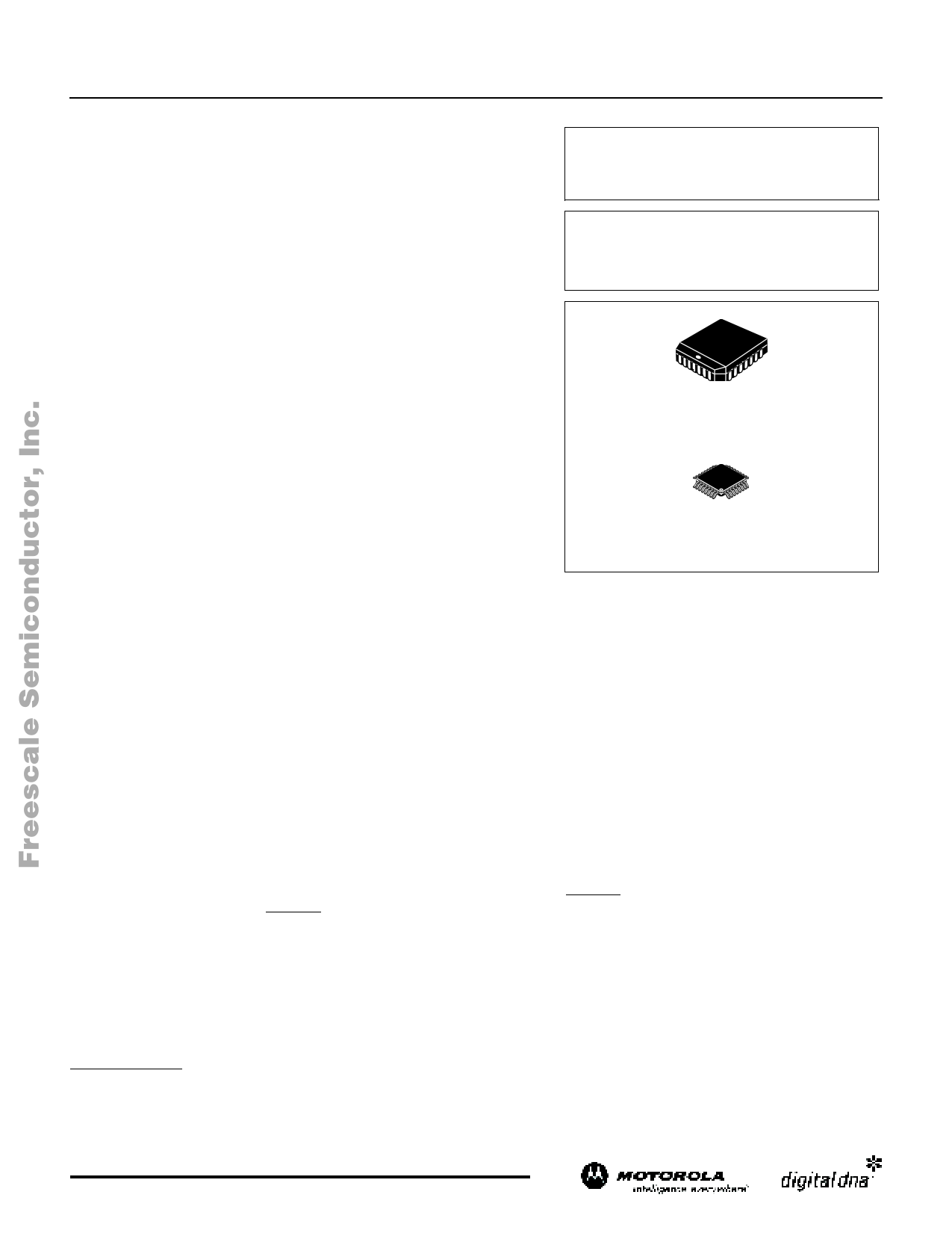
FN SUFFIX
28-LEAD PLCC PACKAGE
CASE 776-02
FA SUFFIX
32-LEAD TQFP PACKAGE
CASE 873A-03
Functional Description
The internal crystal oscillator uses the external quartz crystal as the basis of its frequency reference. The frequency of the internal
crystal oscillator is divided by 16 and then multiplied by the PLL. The VCO within the PLL operates over a range of 800 to 1600 MHz.1
Its output is scaled by a divider that is configured by either the serial or parallel interfaces. The crystal oscillator frequency fXTAL, the
PLL feedback-divider M and the PLL post-divider N determine the output frequency.
The feedback path of the PLL is internal. The PLL adjusts the VCO output frequency to be 8⋅M times the reference frequency by
adjusting the VCO control voltage. Note that for some values of M (either too high or too low) the PLL will not achieve phase lock. The
PLL will be stable if the VCO frequency is within the specified VCO frequency range (800 to 1600 MHz1). The M-value must be pro-
grammed by the serial or parallel interface.
The PLL post-divider N is configured through either the serial or the parallel interfaces, and can provide one of four division ratios
(1, 2, 4, or 8). This divider extends performance of the part while providing a 50% duty cycle. The output driver is driven differentially
from the output divider, and is capable of driving a pair of transmission lines terminated 50Ω to VCC – 2.0V. The positive supply voltage
for the internal PLL is separated from the power supply for the core logic and output drivers to minimize noise induced jitter.
The configuration logic has two sections: serial and parallel. The parallel interface uses the values at the M[8:0] and N[1:0] inputs
to configure the internal counters. It is recommended on system reset to hold the P_LOAD input LOW until power becomes valid. On
the LOW–to–HIGH transition of P_LOAD, the parallel inputs are captured. The parallel interface has priority over the serial interface.
Internal pullup resistors are provided on the M[8:0] and N[1:0] inputs prevent the LVCMOS compatible control inputs from floating.
The serial interface centers on a fourteen bit shift register. The shift register shifts once per rising edge of the S_CLOCK input. The
serial input S_DATA must meet setup and hold timing as specified in the AC Characteristics section of this document. The configura-
tion latches will capture the value of the shift register on the HIGH-to-LOW edge of the S_LOAD input. See the programming section
for more information. The TEST output reflects various internal node values, and is controlled by the T[2:0] bits in the serial data
stream. In order to minimize the PLL jitter, it is recommended to avoid active signal on the TEST output.
1. The VCO frequency range of 800–1600 MHz is available at an ambient temperature range of 0 to 70°C. At –40 to +85°C, the VCO frequency (output
frequency) is limited to max. 1500 MHz (750 MHz)
© Motorola, Inc. 2004
For More Information On This Product,
Go to: www.freescale.com
1 page 
MPC9230
Freescale Semiconductor, Inc.
Table 7. AC Characteristics (VCC = 3.3V ± 5%, TA = –40°C to +85°C)
Symbol
Characteristics
Min Typ Max
LVCMOS Control Inputs (FREF_EXT, XTAL_SEL, P_LOAD, S_LOAD, S_DATA, S_CLOCK, M[0:8], N[0:1]. OE)
VIH Input High Voltage
2.0 VCC + 0.3
VIL Input Low Voltage
0.8
IIN Input Current1
±200
Differential Clock Output FOUT2
VOH
Output High Voltage
VOL Output Low Voltage
VCC–1.1
VCC–1.95
VCC–0.74
VCC–1.65
Test and Diagnosis Output TEST
VOH
Output High Voltage
VOL Output Low Voltage
VCC–1.1
VCC–1.95
VCC–0.74
VCC–1.65
Supply Current
ICC_PLL Maximum PLL Supply Current
ICC Maximum Supply Current
20
110
1. Inputs have pull-down resistors affecting the input current.
2. Outputs terminated 50Ω to VTT = VCC – 2V.
Unit Condition
V LVCMOS
V LVCMOS
µA VIN = VCC or GND
V LVPECL
V LVPECL
V LVPECL
V LVPECL
mA VCC_PLL Pins
mA All VCC Pins
MOTOROLA
5
For More Information On This Product,
Go to: www.freescale.com
TIMING SOLUTIONS
5 Page 
MPC9230
Freescale Semiconductor, Inc.
power and grounds and fully differential PLL), there still may be
applications in which overall performance is being degraded
due to system power supply noise. The power supply filter and
bypass schemes discussed in this section should be adequate
to eliminate power supply noise related problems in most
designs.
C1 C1
1
CF C2
XTAL
= VCC
= GND
= Via
Figure 6. PCB Board Layout Recommendation for
the PLCC28 Package
Using the On-Board Crystal Oscillator
The MPC9230 features a fully integrated on-board crystal
oscillator to minimize system implementation costs. The
oscillator is a series resonant, multivibrator type design as
opposed to the more common parallel resonant oscillator
design. The series resonant design provides better stability and
eliminates the need for large on chip capacitors. The oscillator
is totally self contained so that the only external component
required is the crystal. As the oscillator is somewhat sensitive to
loading on its inputs the user is advised to mount the crystal as
close to the MPC9230 as possible to avoid any board level
parasitics. To facilitate co-location surface mount crystals are
recommended, but not required. Because the series resonant
design is affected by capacitive loading on the XTAL terminals
loading variation introduced by crystals from different vendors
could be a potential issue. For crystals with a higher shunt
capacitance it may be required to place a resistance across the
terminals to suppress the third harmonic. Although typically not
required it is a good idea to layout the PCB with the provision of
adding this external resistor. The resistor value will typically be
between 500 and 1 KΩ.
The oscillator circuit is a series resonant circuit and thus for
optimum performance a series resonant crystal should be used.
Unfortunately most crystals are characterized in a parallel
resonant mode. Fortunately there is no physical difference
between a series resonant and a parallel resonant crystal. The
difference is purely in the way the devices are characterized. As
a result a parallel resonant crystal can be used with the
MPC9230 with only a minor error in the desired frequency. A
parallel resonant mode crystal used in a series resonant circuit
will exhibit a frequency of oscillation a few hundred ppm lower
than specified, a few hundred ppm translates to kHz
inaccuracies. In a general computer application this level of
inaccuracy is immaterial. Table 14 below specifies the
performance requirements of the crystals to be used with the
MPC9230.
Table 14. Recommended Crystal Specifications
Parameter
Value
Crystal Cut
Fundamental AT Cut
Resonance
Series Resonance1
Frequency Tolerance
±75ppm at 25°C
Frequency/Temperature Stability
±150pm 0 to 70°C
Operating Range
0 to 70°C
Shunt Capacitance
5–7pF
Equivalent Series Resistance (ESR) 50 to 80Ω
Correlation Drive Level
100µΩ
Aging
5ppm/Yr (First 3 Years)
1. See accompanying text for series versus parallel resonant
discussion.
MOTOROLA
11
For More Information On This Product,
Go to: www.freescale.com
TIMING SOLUTIONS
11 Page | ||
| Páginas | Total 16 Páginas | |
| PDF Descargar | [ Datasheet MPC9230.PDF ] | |
Hoja de datos destacado
| Número de pieza | Descripción | Fabricantes |
| MPC9230 | 800 MHz Low Voltage PECL Clock Synthesizer | Motorola Semiconductors |
| MPC9230 | 800MHz Low Voltage PECL Clock Synthesizer | IDT |
| MPC9239 | 900 MHz Low Voltage LVPECL Clock Synthesizer | Freescale Semiconductor |
| Número de pieza | Descripción | Fabricantes |
| SLA6805M | High Voltage 3 phase Motor Driver IC. |
Sanken |
| SDC1742 | 12- and 14-Bit Hybrid Synchro / Resolver-to-Digital Converters. |
Analog Devices |
|
DataSheet.es es una pagina web que funciona como un repositorio de manuales o hoja de datos de muchos de los productos más populares, |
| DataSheet.es | 2020 | Privacy Policy | Contacto | Buscar |