|
|
|
PDF MPC92432 Data sheet ( Hoja de datos )
| Número de pieza | MPC92432 | |
| Descripción | 1360 MHz Dual Output LVPECL Clock Synthesizer | |
| Fabricantes | IDT | |
| Logotipo | ||
Hay una vista previa y un enlace de descarga de MPC92432 (archivo pdf) en la parte inferior de esta página. Total 19 Páginas | ||
|
No Preview Available !
Freescale Semiconductor
Technical Data
1C3lo61Sc0k3yM6SnH0ytzhnMtDehHsueiazszlieDzOeruuratpluOt uLVtpPuEtCLLVPECL Clock
DATMAPCS9H2E43E2T
Rev 2, 06/2005
MPC92432
MPC92432
The MPC92432 is a 3.3 V compatible, PLL based clock synthesizer targeted
for high performance clock generation in mid-range to high-performance
telecom, networking, and computing applications. With output frequencies from
21.25 MHz to 1360 MHz and the support of two differential PECL output signals,
the device meets the needs of the most demanding clock applications.
Features
• 21.25 MHz to 1360 MHz synthesized clock output signal
• Two differential, LVPECL-compatible high-frequency outputs
• Output frequency programmable through 2-wire I2C bus or parallel interface
• On-chip crystal oscillator for reference frequency generation
• Alternative LVCMOS compatible reference clock input
• Synchronous clock stop functionality for both outputs
• LOCK indicator output (LVCMOS)
• LVCMOS compatible control inputs
• Fully integrated PLL
• 3.3-V power supply
• 48-lead LQFP
• 48-lead Pb-free package available
• SiGe Technology
• Ambient temperature range: –40°C to +85°C
Applications
• Programmable clock source for server, computing, and telecommunication systems
• Frequency margining
• Oscillator replacement
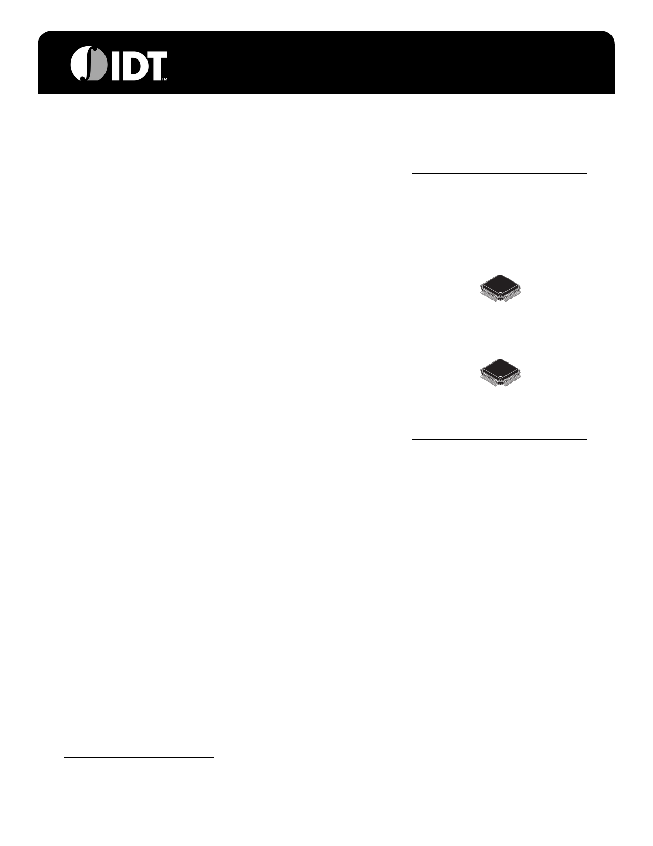
1360 MHz LOW VOLTAGE
CLOCK SYNTHESIZER
FA SUFFIX(1)
48-LEAD LQFP PACKAGE
CASE 932-03
AE SUFFIX(2)
48-LEAD LQFP PACKAGE
Pb-FREE PACKAGE
CASE 932-03
Functional Description
The MPC92432 is a programmable high-frequency clock source (clock synthesizer). The internal PLL generates a high-
frequency output signal based on a low-frequency reference signal. The frequency of the output signal is programmable and can
be changed on the fly for frequency margining purpose.
The internal crystal oscillator uses the external quartz crystal as the basis of its frequency reference. Alternatively, a LVCMOS
compatible clock signal can be used as a PLL reference signal. The frequency of the internal crystal oscillator is divided by a
selectable divider and then multiplied by the PLL. The VCO within the PLL operates over a range of 1360 to 2720 MHz. Its output
is scaled by a divider that is configured by either the I2C or parallel interfaces. The crystal oscillator frequency fXTAL, the PLL pre-
divider P, the feedback-divider M, and the PLL post-divider N determine the output frequency. The feedback path of the PLL is
internal.
The PLL post-divider N is configured through either the I2C or the parallel interfaces, and can provide one of six division ratios
(2, 4, 8, 16, 32, 64). This divider extends the performance of the part while providing a 50% duty cycle. The high-frequency out-
puts, QA and QB, are differential and are capable of driving a pair of transmission lines terminated 50 Ω to VCC – 2.0 V. The second
high-frequency output, QB, can be configured to run at either 1x or 1/2x of the clock frequency or the first output (QA). The positive
supply voltage for the internal PLL is separated from the power supply for the core logic and output drivers to minimize noise
induced jitter.
The configuration logic has two sections: I2C and parallel. The parallel interface uses the values at the M[9:0], NA[2:0], NB,
and P parallel inputs to configure the internal PLL dividers. The parallel programming interface has priority over the serial I2C
interface. The serial interface is I2C compatible and provides read and write access to the internal PLL configuration registers.
The lock state of the PLL is indicated by the LVCMOS-compatible LOCK output.
1. FA suffix: leaded terminations.
2. AE suffix: lead-free, EPP and RoHS-compliant.
IDT™ 1360 MHz Dual Output LVPECL Clock Synthesizer
Freesc©aleFTreimesincgalSeoSluetmioincosnOdrugcatnoirz,aItniocn., h2a0s05b.eAenll raicgqhutsirreedsbeyrvIendte. grated Device Technology, Inc
1
MPC92432
1 page 
MPC92432
1360 MHz Dual Output LVPECL Clock Synthesizer
NETCOM
Table 3. General Specifications
Symbol
Characteristics
VTT Output Termination Voltage
MM ESD Protection (Machine Model)
HBM ESD Protection (Human Body Model)
LU Latch-Up Immunity
CIN Input Capacitance
θJA LQFP 48 Thermal Resistance Junction to Ambient
JESD 51-3, single layer test board
Min
200
2000
200
JESD 51-6, 2S2P multilayer test board
θJC LQFP 48 Thermal Resistance Junction to Case
Typ
VCC – 2
4.0
69
64
53
50
TBD
Max
TBD
Unit
Condition
V
V
V
mA
pF Inputs
°C/W Natural convection
°C/W 200 ft/min
°C/W Natural convection
°C/W 200 ft/min
°C/W MIL-SPEC 883E
Method 1012.1
Table 4. Absolute Maximum Ratings(1)
Symbol
Characteristics
Min
Max
Unit
Condition
VCC Supply Voltage
VIN DC Input Voltage(2)
–0.3
–0.3
3.9
VCC + 0.3
V
V
VOUT
IIN
IOUT
DC Output Voltage
DC Input Current
DC Output Current
–0.3
VCC + 0.3
±20
±50
V
mA
mA
TS Storage Temperature
–65 125 °C
1. Absolute maximum continuous ratings are those maximum values beyond which damage to the device may occur. Exposure to these
conditions or conditions beyond those indicated may adversely affect device reliability. Functional operation at absolute-maximum-rated
conditions is not implied.
2. All input pins including SDA and SCL pins.
IDT™ 1360 MHz Dual Output LVPECL Clock Synthesizer
FreescalAedTviamnicnegdSCollouctikonDsrivOerrgsaDniezvaitcioens has been acquired by Integrated Device Technology, Inc
Freescale Semiconductor
5
MPC924M32PC92432
5
5 Page 
MPC92432
1360 MHz Dual Output LVPECL Clock Synthesizer
NETCOM
Programming the I2C Interface
Table 18. I2C Slave Address
Bit 7 6 5 4 3
2
1
0
Value 1 0 1 1 0 Pin Pin R/W
ADR1 ADR0
The 7-bit I2C slave address of the MPC92432 synthesizer
is a combination of a 5-bit fixed addresses and two variable
bits which are set by the hardware pins ADR[1:0]. Bit 0 of the
MPC92432 slave address is used by the bus controller to
select either the read or write mode. ’0’ indicates a
transmission (I2C-WRITE) to the MPC92432. ’1’ indicates a
request for data (I2C-READ) from the synthesizer. The
hardware pins ADR1 and ADR0 and should be individually
set by the user to avoid address conflicts of multiple
MPC92432 devices on the same I2C bus.
Write Mode (R/W = 0)
The configuration registers are written by the bus
controller by the initiation of a write transfer with the
MPC92432 slave address (first byte), followed by the address
of the configuration register (second byte: 0x00, 0x01 or
0xF0), and the configuration data byte (third byte). This
transfer may be followed by writing more registers by sending
the configuration register address followed by one data byte.
Each byte sent by the bus controller is acknowledged by the
MPC92432. The transfer ends by a stop bit sent by the bus
controller. The number of configuration data bytes and the
write sequence are not restricted.
Table 19. Complete Configuration Register Write Transfer
1 bit
Start
Master
7 bits
Slave address
10110xx(1)
Master
1 bit
R/W
0
Mast
1 bit
ACK
Slave
8 bits
&PLL_H
0x01
Master
1 bit
ACK
8 bits
Config-Byte 1
Data
1 bit
ACK
Slave
Master
Slave
1. xx = state of ADR1, ADR0 pins
8 bits
&PLL_L
0x00
Master
1 bit
ACK
8 bits
Config-Byte 2
Data
1 bit
ACK
1 bit
Stop
Slave Master Slave Mast
Read Mode (R/W = 1)
The configuration registers are read by the bus controller
by the initiation of a read transfer. The MPC92432 supports
read transfers immediately after the first byte without a
change in the transfer direction. Immediately after the bus
controller sends the slave address, the MPC92432
acknowledges and then sends both configuration register
PLL_L and PLL_H (back-to-back) to the bus controller. The
CMD register cannot be read. In order to read the two
synthesizer registers and the current PLL configuration
setting, the user can 1) read PLL_L, PLL_H, write the GET
command (loads the current configuration into PLL_L,
PLL_H) and read PLL_L, PLL_H again. Note that the PLL_L,
PLL_H registers and divider settings may not be equivalent
after the following cases:
a. Writing the INC command
b. Writing the DEC command
c. Writing PLL_L, PLL_H registers with a new
configuration and not writing the LOAD command.
Table 20. Configuration Register Read Transfer
1 bit
Start
Master
7 bits
Slave address
10110xx(1)
Master
1 bit
R/W
1
Mast
1. xx = state of ADR1, ADR0 pins
1 bit
ACK
Slave
Device Startup
General Device Configuration
It is recommended to reset the MPC92432 during or
immediately after the system powers up (MR = 0). The device
acquires an initial PLL divider configuration through the
parallel interface pins M[9:0], NA[2:0], N, and P(1) with the
low-to-high transition of MR(2). PLL frequency lock is
8 bits
PLL_L
Data
Slave
1 bit
ACK
Mast
8 bits
PLL_H
Data
Slave
1 bit
ACK
Master
1 bit
Stop
Slave
achieved within the specified lock time (tLOCK) and is
indicated by an assertion of the LOCK signal which
completes the startup procedure. It is recommended to
disable the outputs (CLK_STOPx = 0) until PLL lock is
achieved to suppress output frequency transitions. The
output frequency can be reconfigured at any time through
either the parallel or the serial interface.
1. The parallel interface pins M[9:0], NA[2:0], N, and P may be left open (floating). In this case the initial PLL configuration will have the default
setting of M = 500, P = 1, NA[2:0] = 010, NB = 0, resulting in an internal VCO frequency of 2000 MHz (fref = 16 MHz) and an output frequency
of 250 MHz.
2. The initial PLL configuration is independent on the selected programming mode (PLOAD low or high)
IDT™ 1360 MHz Dual Output LVPECL Clock Synthesizer
FreescalAedTviamnicnegdSCollouctikonDsrivOerrgsaDniezvaitcioens has been acquired by Integrated Device Technology, Inc
Freescale Semiconductor
11
MPC924M32PC92432
11
11 Page | ||
| Páginas | Total 19 Páginas | |
| PDF Descargar | [ Datasheet MPC92432.PDF ] | |
Hoja de datos destacado
| Número de pieza | Descripción | Fabricantes |
| MPC92432 | 1360 MHz Dual Output LVPECL Clock Synthesizer | Motorola Semiconductors |
| MPC92432 | 1360 MHz Dual Output LVPECL Clock Synthesizer | IDT |
| MPC92433 | 1428 MHz Dual Output LVPECL Clock Synthesizer | Freescale Semiconductor |
| MPC92439 | LVPECL Clock Syntheesizer | IDT |
| Número de pieza | Descripción | Fabricantes |
| SLA6805M | High Voltage 3 phase Motor Driver IC. |
Sanken |
| SDC1742 | 12- and 14-Bit Hybrid Synchro / Resolver-to-Digital Converters. |
Analog Devices |
|
DataSheet.es es una pagina web que funciona como un repositorio de manuales o hoja de datos de muchos de los productos más populares, |
| DataSheet.es | 2020 | Privacy Policy | Contacto | Buscar |