|
|
|
PDF LTM10C313U Data sheet ( Hoja de datos )
| Número de pieza | LTM10C313U | |
| Descripción | LCD Module | |
| Fabricantes | Toshiba | |
| Logotipo | ||
Hay una vista previa y un enlace de descarga de LTM10C313U (archivo pdf) en la parte inferior de esta página. Total 10 Páginas | ||
|
No Preview Available !
LIQUID CRYSTAL DISPLAY DIVISION
PRODUCT INFORMATION
FEATURES
(1) 10.4”XGA display size for notebook PC
(2) LVDS interface system
(3) Slim(5.7mmMAX) & light weight design
26cm COLOUR TFT-LCD MODULE
(10.4 TYPE)
LTM10C313U
(p-Si TFT)
XGA
TENTATIVE
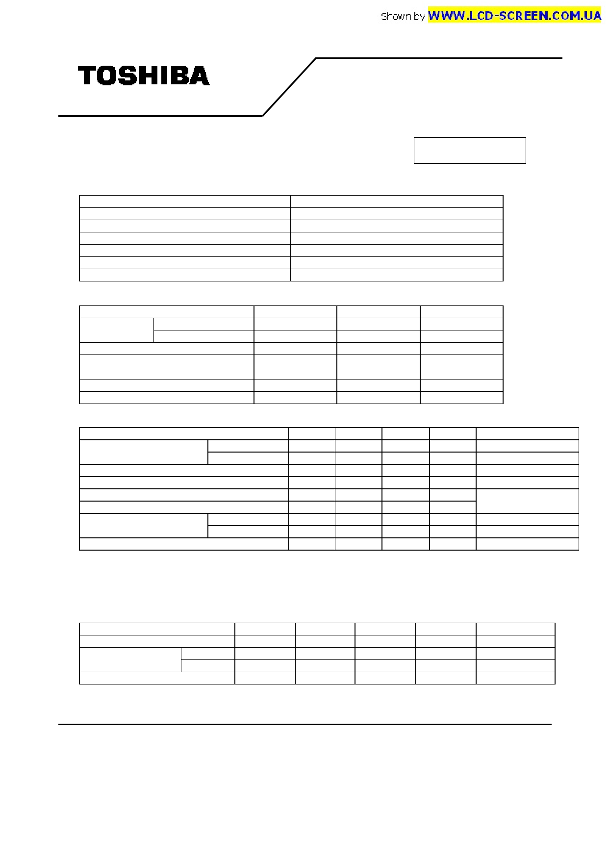
MECHANICAL SPECIFICATIONS
Item
Dimensional Outline (Typ.)
Number of Pixels
Active Area
Pixel Pitch
Weight (approximately)
Backlight
Specifications
238.6(W) x 173.2(H) x 5.7max(D) mm
1024(W) x 768(H) pixels
210.432(W) x 157.824(H) mm
0.2055(W) x 0.2055(H)
270 g
Single CCFL, Sidelight type
ABSOLUTE MAXIMUM RATINGS
Item
Supply Voltage (VDD)
(VFL)
FL Driving Frequency (fFL)
Input Signal Voltage (VIN)
Operating Temperature
Storage Temperature
Storage Humidity
Min. Max. Unit
-0.3 4.0
V
0 2.0 kV(rms)
- 100 kHz
-0.3 VDD+0.3
0 50
-20 60
V
°C
°C
10 90 %(RH)
ELECTRICAL SPECIFICATION
Item
Min. Typ. Max. Unit
Remarks
Supply Voltage
FL Start Voltage (Ta=0°C)
(VDD)
(VFL)
3.0 3.3 3.6
V
540 590 640 V(rms) IFL=5 mA(rms)
1200 --- 1600 V(rms)
Receiver Input Voltage
0
--- 2.4
V
Differential Input High Threshold(VTH)*1
Differential Input Low Threshold(VTL)*1
Current Consumption
*2 (IDD)
*3 (IFL)
*2 *3 Power Consumption
---
VOS-0.1
---
3.0
---
--- VOS+0.1
V VOS:Offset Mode Voltage
--- --- V VOS=+1.2V
230 --- mA(rms)
5.0 6.0 mA(rms)
3.7 --- W
*1 : Refer to DF90CF364 Specification by National Semiconductor Corporation. This LCD module conforms to LVDS
standard (TIA/EIA-644)
*2 : 8 color bars pattern
*3 : Excepting the efficiency FL inverter
*4 : Not use Hsync nor Vsync. Only ENAB control.
OPTICAL SPECIFICATION (Ta=25°C)
Item Min. Typ. Max. Unit Remarks
Contrast Ratio (CR)
100 250
---
---
Response Time
Luminance (L)
(tON)
(tOFF)
--- --- 50 ms
--- --- 50 ms
--- 150
---
cd/m 2
I FL=5mA( r m s )
*The information contained herein is presented only as a guide for the applications of our products. No responsibility is assumed by
Toshiba or other rights of the third parties which may result from its use. No license is granted by implication or otherwise under any
patent or patent rights of Toshiba or others.
*The information contained herein may be changed without prior notice. It is therefore advisable to contact Toshiba before proceeding
with the design of equipment incorporating this product.
(1/10)
2002-01-09 (Ver.0.2)
1 page 
LTM10C313U
TIMING SPECIFICATION 2) 3) 4)
Item
Frame Period
Vertical
Display Term
One Line Scanning
Time
Horizontal
Display Term
Clock Period
Symbol
t1
t2
t3
t4
t5
Min.
778 x t3
768 x t3
1336 x t5
20.04
1024 x t5
15.0
Typ.
806 x t3
16.67
768 x t3
1344 x t5
20.68
1024 x t5
15.38
Max.
860 x t3
17.78
768 x t3
1462 x t5
---
1024 x t5
---
Unit Remarks
--- 1) 5)
ms
--- 1) 5)
--- 1) 5)
ms
--- 1) 6)
ns
Note 1) Refer to TIMING CHART at page4 and LVDS specification (DS90CF364) by National Semiconductor Corporation.
Note 2) If ENAB is fixed to "H" or "L" level for certain period while NCLK is supplied, the panel displays black with some
flicker.
Note 3) Don't fix NCLK to "H" or "L" level while the VDD(+3.3V) is supplied.
If NCLK is fixed to "H" or "L" level for certain period while ENAB is spplied, the panel may be damaged.
When It holds on, DC voltage supplies to liquid crystal materials and It may cause damage to liquid crystal materials.
Graphic controller 69000 (Chips & Technology), for example, causes above phenomenon
Note 4) Please adjust LCD operating signal timing and FL driving frequency, to optimize the display quality.
There is a possibility that flicker is observed by the interference of LCD operating signal timing and FL driving condition
(especially driving frequency), even if the condition satisfies above timing specifications and recommended operating
conditions shown in 3.
Note 5) Do not make t1, t2 and t3 fluctuate.
If t1, t2 and t3 are fluctuate, the panel displays black.
Note 6) Keep constant the number of clock within one line scanning time and the number of scanning line within one flame
period
SEQUENCE OF POWER SUPPLIES AND SIGNALS
(5/10)
2002-01-09 (Ver.0.2)
5 Page | ||
| Páginas | Total 10 Páginas | |
| PDF Descargar | [ Datasheet LTM10C313U.PDF ] | |
Hoja de datos destacado
| Número de pieza | Descripción | Fabricantes |
| LTM10C313K | LCD Module | Toshiba |
| LTM10C313U | LCD Module | Toshiba |
| Número de pieza | Descripción | Fabricantes |
| SLA6805M | High Voltage 3 phase Motor Driver IC. |
Sanken |
| SDC1742 | 12- and 14-Bit Hybrid Synchro / Resolver-to-Digital Converters. |
Analog Devices |
|
DataSheet.es es una pagina web que funciona como un repositorio de manuales o hoja de datos de muchos de los productos más populares, |
| DataSheet.es | 2020 | Privacy Policy | Contacto | Buscar |