|
|
PDF AT40K40 Data sheet ( Hoja de datos )
| Número de pieza | AT40K40 | |
| Descripción | 5K - 50K Gates Coprocessor FPGA | |
| Fabricantes | ATMEL Corporation | |
| Logotipo |  |
|
Hay una vista previa y un enlace de descarga de AT40K40 (archivo pdf) en la parte inferior de esta página. Total 30 Páginas | ||
|
No Preview Available !
AT40K05, AT40K10, AT40K20, AT40K40
5K – 50K Gates Coprocessor FPGA with FreeRAM™
Features
DATASHEET
Ultra high performance
System speeds to 100MHz
Array multipliers > 50MHz
10ns flexible SRAM
Internal tri-state capability in each cell
FreeRAM™
Flexible, single/dual port, synchronous/asynchronous 10ns SRAM
2,048 – 18,432 bits of distributed SRAM independent of logic cells
128 – 384 PCI compliant I/Os
5V capability
Programmable output drive
Fast, flexible array access facilitates pin locking
Pin-compatible with XC4000 and XC5200 FPGAs
Eight global clocks
Fast, low skew clock distribution
Programmable rising/falling edge transitions
Distributed clock shutdown capability for low power management
Global reset/asynchronous reset options
4 additional dedicated PCI clocks
Cache Logic® dynamic full/partial re-configurability in-system
Unlimited re-programmability via serial or parallel modes
Enables adaptive designs
Enables fast vector multiplier updates
Pin-compatible package options
Thin, Plastic Quad Flat Packs (LQFP and PQFP)
User-friendly design tools
Timing driven placement and routing
Automatic/Interactive multi-chip partitioning
Fast, efficient synthesis
Over 75 automatic component generators create 1000s of reusable, Fully
Deterministic Logic and RAM functions
Intellectual property cores
Fir Filters, UARTs, PCI, FFT, and other system level functions
Supply voltage 5V for AT40K
Atmel-0896E-FPGA-AT40K05-10-20-40-Datasheet_062013
1 page 
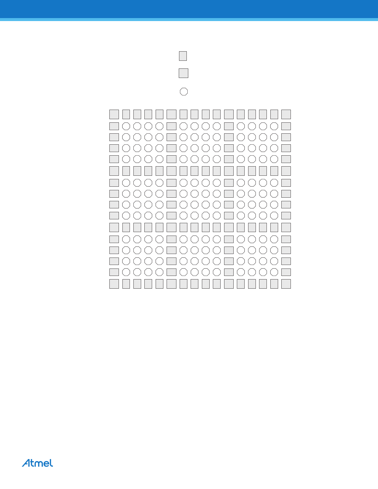
Figure 2-2. Floor Plan (Representative Portion)(1)
RV = Vertical Repeater
RH = Horizontal Repeater
= Core Cell
RAM RV RV RV RV RAM RV RV RV RV RAM RV RV RV RV RAM
RH RH RH RH
RH RH RH RH
RH RH RH RH
RH RH RH RH
RAM RV RV RV RV RAM RV RV RV RV RAM RV RV RV RV RAM
RH RH RH RH
RH RH RH RH
RH RH RH RH
RH RH RH RH
RAM RV RV RV RV RAM RV RV RV RV RAM RV RV RV RV RAM
RH RH RH RH
RH RH RH RH
RH RH RH RH
RH RH RH RH
RAM RV RV RV RV RAM RV RV RV RV RAM RV RV RV RV RAM
Note:
1. Repeaters regenerate signals and can connect any bus to any other bus (all pathways are legal) on the
same plane. Each repeater has connections to two adjacent local-bus segments and two express-bus
segments. This is done automatically using the Integrated Development System (IDS) tool.
Atmel AT40K Series FPGA [DATASHEET]
Atmel-0896E-FPGA-AT40K05-10-20-40-Datasheet_062013
5
5 Page 
6. RAM
32 x 4 dual-ported RAM blocks are dispersed throughout the array, see Figure 6-1. A 4-bit Input Data Bus connects to
four horizontal local buses distributed over four sector rows (Plane 1). A 4-bit Output Data Bus connects to four horizontal
local buses distributed over four sectors in the same column. A 5-bit Output Address Bus connects to five vertical
express buses in the same column. Ain (input address) and Aout (output address) alternate positions in horizontally
aligned RAM blocks. For the left-most RAM blocks, Aout is on the left and Ain is on the right. For the right-most RAM
blocks, Ain is on the left and Aout is tied off, thus it can only be configured as a single port. For single-ported RAM, Ain is
the READ/WRITE address port and Din is the (bi-directional) data port. Right-most RAM blocks can be used only for
single-ported memories. WEN and OEN connect to the vertical express buses in the same column.
Figure 6-1. RAM Connections (One Ram Block)
CLK
CLK
CLK
CLK
Din Dout
Ain Aout
32 x 4 RAM
WEN
OEN CLK
Reading and writing of the 10ns 32 x 4 dual-port FreeRAM are independent of each other. Reading the 32 x 4 dual-port
RAM is completely asynchronous. Latches are transparent; when Load is Logic 1, data flows through; when Load is
Logic 0, data is latched. These latches are used to synchronize Write Address, Write Enable Not, and Din signals for a
synchronous RAM. Each bit in the 32 x 4 dual-port RAM is also a transparent latch. The front-end latch and the memory
latch together form an edge-triggered flip flop. When a nibble (bit = 7) is (Write) addressed and LOAD is Logic 1 and WE
is Logic 0, data flows through the bit. When a nibble is not (Write) addressed or LOAD is logic 0 or WE is Logic 1, data is
latched in the nibble. The two CLOCK muxes are controlled together; they both select CLOCK (for a synchronous RAM)
or they both select “1” (for an asynchronous RAM). CLOCK is obtained from the clock for the sector-column immediately
to the left and immediately above the RAM block. Writing any value to the RAM clear byte during configuration clears the
RAM (see the “AT40K Configuration Series” application note at www.atmel.com).
Atmel AT40K Series FPGA [DATASHEET]
Atmel-0896E-FPGA-AT40K05-10-20-40-Datasheet_062013
11
11 Page | ||
| Páginas | Total 30 Páginas | |
| PDF Descargar | [ Datasheet AT40K40.PDF ] | |
Hoja de datos destacado
| Número de pieza | Descripción | Fabricantes |
| AT40K40 | 5K - 50K Gates Coprocessor FPGA | ATMEL Corporation |
| Número de pieza | Descripción | Fabricantes |
| SLA6805M | High Voltage 3 phase Motor Driver IC. |
Sanken |
| SDC1742 | 12- and 14-Bit Hybrid Synchro / Resolver-to-Digital Converters. |
Analog Devices |
|
DataSheet.es es una pagina web que funciona como un repositorio de manuales o hoja de datos de muchos de los productos más populares, |
| DataSheet.es | 2020 | Privacy Policy | Contacto | Buscar |
