|
|
|
PDF MT8962 Data sheet ( Hoja de datos )
| Número de pieza | MT8962 | |
| Descripción | Integrated PCM Filter Codec | |
| Fabricantes | Zarlink Semiconductor | |
| Logotipo | ||
Hay una vista previa y un enlace de descarga de MT8962 (archivo pdf) en la parte inferior de esta página. Total 30 Páginas | ||
|
No Preview Available !
ISO2-CMOS MT8960/61/62/63/64/65/66/67
Integrated PCM Filter Codec
Data Sheet
Features
• ST-BUS compatible
• Transmit/Receive filters & PCM Codec in one I.C
• Meets AT&T D3/D4 and CCITT G711 and G712
• µ-Law: MT8960/62/64/67
• A-Law: MT8961/63/65/67
• Low power consumption:
Op.: 30 mW typ.
Stby.: 2.5 mW typ.
• Digital Coding Options:
MT8964/65/66/67 CCITT Code
MT8960/61/62/63 Alternative Code
• Digitally controlled gain adjust of both filters
• Analog and digital loopback
• Filters and codec independently user accessible
for testing
• Powerdown mode available
• 2.048 MHz master clock input
• Up to six uncommitted control outputs
• ±5 V ±5% power supply
February 2005
Ordering Information
MT8960/61/64/65AE
MT8962/63AE
MT8962/63/66/67AS
MT8963ASR
MT8960AE1
MT8962/63AE1
MT8962AS1
MT8963AS1
18 Pin PDIP
20 Pin PDIP
20 Pin SOIC
20 Pin SOIC
18 Pin PDIP*
20 Pin PDIP*
20 Pin SOIC*
20 Pin SOIC*
*Pb Free Matte Tin
-40°C to +85°C
Tubes
Tubes
Tubes
Tape & Reel
Tubes
Tubes
Tubes
Tubes
Description
Manufactured in ISO2-CMOS, these integrated
filter/codecs are designed to meet the demanding
performance needs of the digital telecommunications
industry, e.g., PABX, Central Office, Digital telephones.
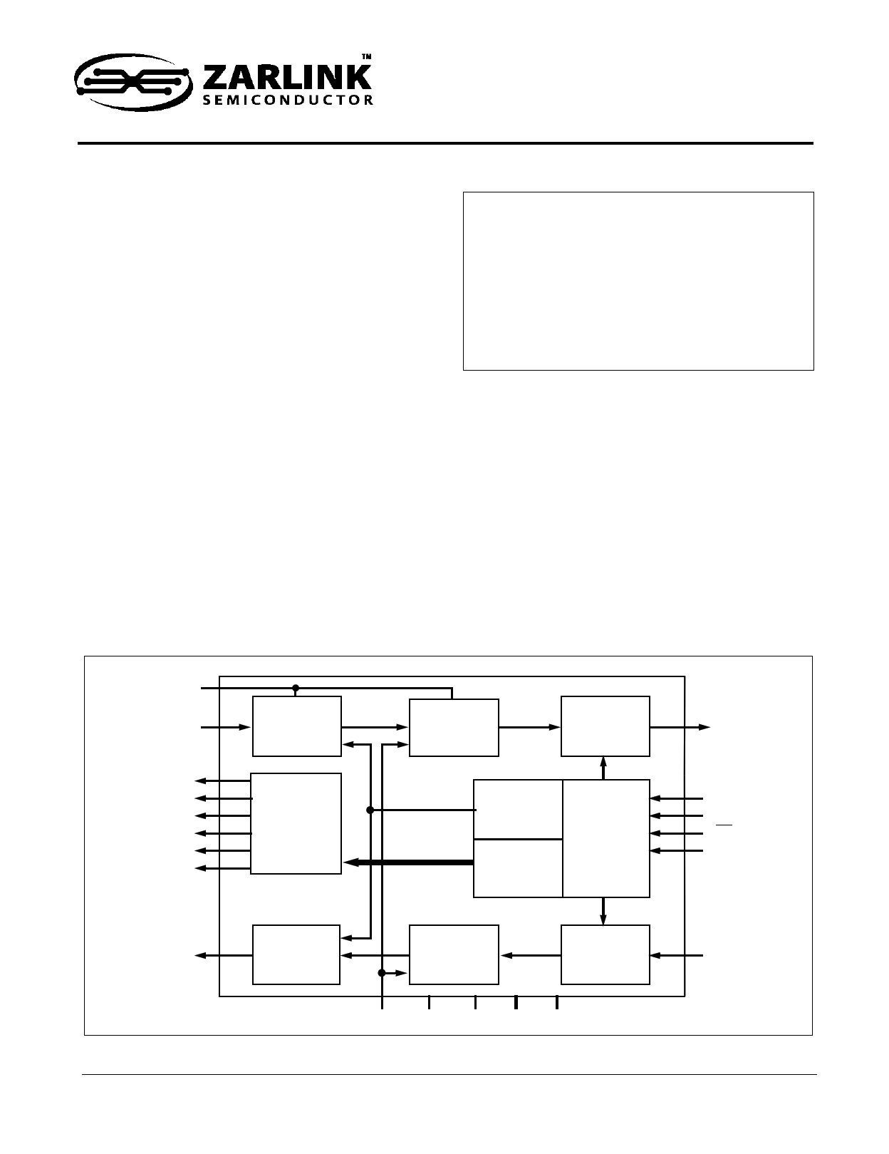
ANUL
VX
SD0
SD1
SD2
SD3
SD4
SD5
Transmit
Filter
Output
Register
Analog to
Digital PCM
Encoder
Output
Register
A Register
8-Bits
B-Register
8-Bits
Control
Logic
DSTo
CSTi
CA
F1i
C2i
VR
Receive
Filter
PCM Digital
to Analog
Decoder
Input
Register
DSTi
VRef GNDA GNDD VDD VEE
Figure 1 - Functional Block Diagram
1
Zarlink Semiconductor Inc.
Zarlink, ZL and the Zarlink Semiconductor logo are trademarks of Zarlink Semiconductor Inc.
Copyright 2003-2005, Zarlink Semiconductor Inc. All Rights Reserved.
1 page 
MT8960/61/62/63/64/65/66/67
Data Sheet
injects this voltage level into the non-inverting input of the comparator. An integrating capacitor (of value between
0.1 and 1 µF) must be externally connected from this point (ANUL) to the Analog Ground (GNDA).
The absolute gain of the transmit filter (nominally 0 dB at 1 kHz) can be adjusted from 0 dB to 7 dB in 1 dB steps by
means of three binary controlled gain pads.
The resulting bandpass characteristics with the limits shown in Figure 10 meet the CCITT and AT&T recommended
specifications. Typical attenuations are 30 dB for 0-60 Hz and 35 dB for 4.6 kHz and above.
The filter output signal is an 8 kHz staircase waveform which is fed into the codec capacitor array, or alternatively,
into an external capacitive load of 250 pF when the chip is in the test mode. The digital encoder generates an eight-
bit digital word representation of the 8 kHz sampled analog signal. The first bit of serial data stream is bit 7 (MSB)
and represents the sign of the analog signal. Bits 4-6 represent the chord which contains the analog sample value.
Bits 0-3 represent the step value of the analog sample within the selected chord. The MT8960-63 provide a sign
plus magnitude PCM output code format. The MT8964/66 PCM output code conforms to the AT &T D3
specification, i.e., true sign bit and inverted magnitude bits. The MT8965/67 PCM output code conforms to the
CCITT specifications with alternate digit inversion (even bits inverted). See Figs. 3 and 4 for the digital output code
corresponding to the analog voltage, VIN, at VX input.
The eight-bit digital word is output at DSTo at a nominal rate of 2.048 MHz, via the output buffer as the first 8-bits of
the 125 µs sampling frame.
Receive Path
An eight-bit PCM encoded digital word is received on DSTi input once during the 125 µs period and is loaded into
the input register. A charge proportional to the received PCM word appears on the capacitor array and an 8 kHz
sample and hold circuit integrates this charge and holds it for the rest of the sampling period.
The receive (D/A) filter provides interpolation filtering on the 8 kHz sample and hold signal from the codec. The filter
consists of a 3.4 kHz lowpass fifth-order elliptic section clocked at 128 kHz and performs bandlimiting and
smoothing of the 8 kHz "staircase" waveform. In addition, sinx/x gain correction is applied to the signal to
compensate for the attenuation of higher frequencies caused by the capacitive sample and hold circuit. The
absolute gain of the receive filter can be adjusted from 0 dB to -7 dB in 1 dB steps by means of three binary
controlled gain pads. The resulting lowpass characteristics, with the limits shown in Figure 11, meet the CCITT and
AT & T recommended specifications.
Typical attenuation at 4.6 kHz and above is 30 dB. The filter is followed by a buffer amplifier which will drive 5V
peak/peak into a 10k ohm load, suitable for driving electronic 2-4 wire circuits.
VRef
An external voltage must be supplied to the VRef pin which provides the reference voltage for the digital encoding
and decoding of the analog signal. For VRef = 2.5 V, the digital encode decision value for overload (maximum
analog signal detect level) is equal to an analog input VIN = 2.415 V (µ-Law version) or 2.5 V (A-Law version) and is
equivalent to a signal level of 3.17 dBm0 or 3.14 dBm0 respectively, at the codec.
The analog output voltage from the decoder at VR is defined as:
µ-Law:
VX
[( ) ( )( )]Ref
-0.5
128
+
2C
128
16.5 + S
33
±VOFFSET
A-Law:
[( )( )]V X
Ref
2C+1
128
0.5 + S
32
±VOFFSETC=0
5
Zarlink Semiconductor Inc.
5 Page 
MT8960/61/62/63/64/65/66/67
Data Sheet
BITS 0-2
01
10
11
LOGIC CONTROL OUTPUTS SD0-SD2
Transmit filter testing, i.e.:
Transmit filter input connected to VX input
Receive filter and Buffer disconnected from VR
Receive filter testing, i.e.:
Receive filter input connected to VX input
Receive filter input disconnected from codec
Codec testing i.e.:
Codec analog input connected to VX
Codec analog input disconnected from transmit filter output
Codec analog output connected to VR
VR disconnected from receive filter output
Table 3 - Control States - Register B
Powerdown
Powerdown of the chip is achieved in several ways:
Internal Control:
1) Initial Power-up. Initial application of VDD and VEE causes powerdown for a period of 25 clock cycles and
during this period the chip will accept input only from C2i. The B-register is reset to zero forcing SD0-5 to
be inactive. Bits 0-5 of Register A (gain adjust bits) are forced to zero and bits 6 and 7 of Register A
become logic high thus reinforcing the powerdown.
2) Loss of C2i. Powerdown is entered 10 to 40 µs after C2i has assumed a continuous logic high (VDD). In
this condition the chip will be in the same state as in (1) above.
Note: If C2i stops at a continuous logic low (GNDD), the digital data and status is indeterminate.
External Control:
1) Register A. Powerdown is controlled by bits 6 and 7 (when both at logic high) of Register A which in turn
receives its control word input via CSTi, when F1i is low and CA input is either at VEE or GNDD. Power is
removed from the filters and analog sections of the chip. The analog output buffer at VR will be connected
to GNDA. DSTo becomes high impedance and the clocks to the majority of the logic are stopped. SD
outputs are unaffected and may be updated as normal.
2) CSTi Input. With CA at VEE and CSTi held at continuous logic high the chip assumes the same state as
described in External Control (1) above.
11
Zarlink Semiconductor Inc.
11 Page | ||
| Páginas | Total 30 Páginas | |
| PDF Descargar | [ Datasheet MT8962.PDF ] | |
Hoja de datos destacado
| Número de pieza | Descripción | Fabricantes |
| MT8960 | Integrated PCM Filter Codec | Mitel Networks Corporation |
| MT8960 | Integrated PCM Filter Codec | Zarlink Semiconductor |
| MT8961 | Integrated PCM Filter Codec | Mitel Networks Corporation |
| MT8961 | Integrated PCM Filter Codec | Zarlink Semiconductor |
| Número de pieza | Descripción | Fabricantes |
| SLA6805M | High Voltage 3 phase Motor Driver IC. |
Sanken |
| SDC1742 | 12- and 14-Bit Hybrid Synchro / Resolver-to-Digital Converters. |
Analog Devices |
|
DataSheet.es es una pagina web que funciona como un repositorio de manuales o hoja de datos de muchos de los productos más populares, |
| DataSheet.es | 2020 | Privacy Policy | Contacto | Buscar |