|
|
PDF K4A4G085WD Data sheet ( Hoja de datos )
| Número de pieza | K4A4G085WD | |
| Descripción | 4Gb D-die DDR4 SDRAM | |
| Fabricantes | Samsung | |
| Logotipo |  |
|
Hay una vista previa y un enlace de descarga de K4A4G085WD (archivo pdf) en la parte inferior de esta página. Total 30 Páginas | ||
|
No Preview Available !
Rev. 1.1, Feb. 2014
K4A4G045WD
K4A4G085WD
4Gb D-die DDR4 SDRAM
78FBGA with Lead-Free & Halogen-Free
(RoHS compliant)
1.2V
datasheet
SAMSUNG ELECTRONICS RESERVES THE RIGHT TO CHANGE PRODUCTS, INFORMATION AND
SPECIFICATIONS WITHOUT NOTICE.
Products and specifications discussed herein are for reference purposes only. All information discussed
herein is provided on an "AS IS" basis, without warranties of any kind.
This document and all information discussed herein remain the sole and exclusive property of Samsung
Electronics. No license of any patent, copyright, mask work, trademark or any other intellectual property
right is granted by one party to the other party under this document, by implication, estoppel or other-
wise.
Samsung products are not intended for use in life support, critical care, medical, safety equipment, or
similar applications where product failure could result in loss of life or personal or physical harm, or any
military or defense application, or any governmental procurement to which special terms or provisions
may apply.
For updates or additional information about Samsung products, contact your nearest Samsung office.
All brand names, trademarks and registered trademarks belong to their respective owners.
(C) 2014 Samsung Electronics Co., Ltd. All rights reserved.
-1-
1 page 
K4A4G045WD
K4A4G085WD
datasheet
3. Package pinout/Mechanical Dimension & Addressing
3.1 x4 Package Pinout (Top view) : 78ball FBGA Package
Rev. 1.1
DDR4 SDRAM
12
A
VDD
VSSQ
B
VPP
VDDQ
C VDDQ DQ0
D VSSQ
NC
E
VSS
VDDQ
F VDD
NC
G VSS
NC
H
VDD
WE_n
A14
J VREFCA BG0
K VSS BA0
L RESET_n
A6
M VDD
A8
N VSS A11
3
NC
DQS_c
DQS_t
DQ2
NC
ODT
CKE
ACT_n
A10
AP
A4
A0
A2
PAR
456
7
NC
DQ1
VDD
DQ3
NC
CK_t
CS_n
CAS_n
A15
A12
BC_n
A3
A1
A9
NC
89
VSSQ
VDDQ
VSS
NC
VDDQ
CK_c
NC
RAS_n
VSS
ZQ
VDDQ
VSSQ
VSS
VDD
NC
VSS
BG1
BA1
A5
A7
A13
VDD
VSS
ALERT_n
VPP
VDD
A
B
C
D
E
F
G
H
J
K
L
M
N
Ball Locations (x4)
Populated ball
Ball not populated
Top view
(See the balls through the package)
123456789
A
B
C
D
E
F
G
H
J
K
L
M
N
-5-
5 Page 
K4A4G045WD
K4A4G085WD
datasheet
Rev. 1.1
DDR4 SDRAM
6. Absolute Maximum Ratings
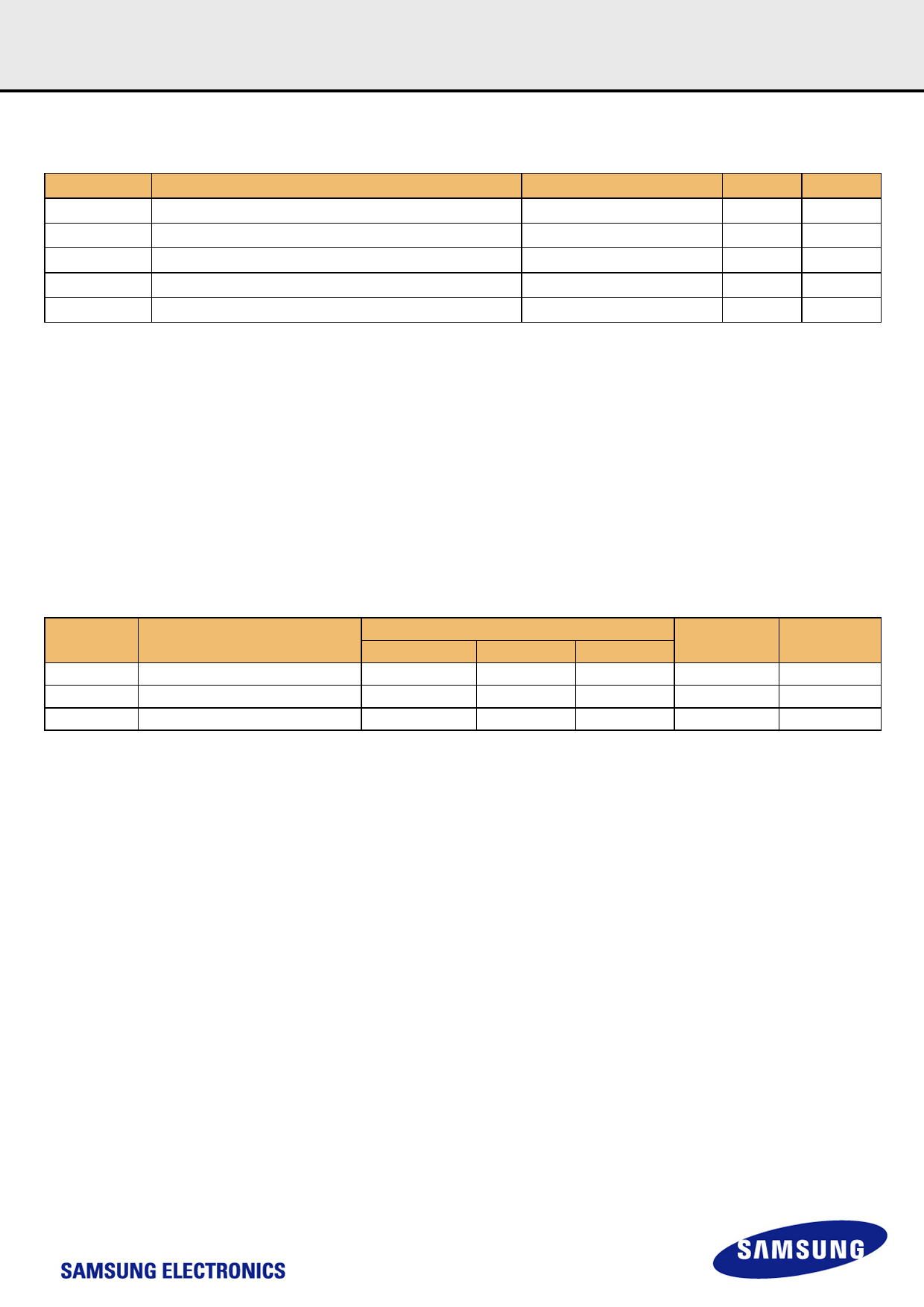
[ Table 4 ] Absolute Maximum DC Ratings
Symbol
Parameter
VDD
Voltage on VDD pin relative to Vss
VDDQ
Voltage on VDDQ pin relative to Vss
VPP
Voltage on VPP pin relative to Vss
VIN, VOUT
Voltage on any pin except VREFCA relative to Vss
TSTG
Storage Temperature
Rating
-0.3 ~ 1.5
-0.3 ~ 1.5
-0.3 ~ 3.0
-0.3 ~ 1.5
-55 to +100
Units
V
V
V
V
°C
NOTE
1,3
1,3
4
1,3,5
1,2
NOTE :
1. Stresses greater than those listed under “Absolute Maximum Ratings” may cause permanent damage to the device. This is a stress rating only and functional operation of the
device at these or any other conditions above those indicated in the operational sections of this specification is not implied. Exposure to absolute maximum rating conditions
for extended periods may affect reliability
2. Storage Temperature is the case surface temperature on the center/top side of the DRAM. For the measurement conditions, please refer to JESD51-2 standard.
3. VDD and VDDQ must be within 300 mV of each other at all times;and VREFCA must be not greater than 0.6 x VDDQ, When VDD and VDDQ are less than 500 mV; VREFCA
may be equal to or less than 300 mV
4. VPP must be equal or greater than VDD/VDDQ at all times.
5. Overshoot area above 1.5 V is specified in section 8.3.4 , 8.3.5 and 8.3.6.
7. AC & DC Operating Conditions
[ Table 5 ] Recommended DC Operating Conditions
Symbol
VDD
VDDQ
VPP
Parameter
Supply Voltage
Supply Voltage for Output
Min.
1.14
1.14
2.375
Rating
Typ.
1.2
1.2
2.5
NOTE :
1. Under all conditions VDDQ must be less than or equal to VDD.
2. VDDQ tracks with VDD. AC parameters are measured with VDD and VDDQ tied together.
3. DC bandwidth is limited to 20MHz.
Max.
1.26
1.26
2.75
Unit
V
V
V
NOTE
1,2,3
1,2,3
3
- 11 -
11 Page | ||
| Páginas | Total 30 Páginas | |
| PDF Descargar | [ Datasheet K4A4G085WD.PDF ] | |
Hoja de datos destacado
| Número de pieza | Descripción | Fabricantes |
| K4A4G085WD | 4Gb D-die DDR4 SDRAM | Samsung |
| Número de pieza | Descripción | Fabricantes |
| SLA6805M | High Voltage 3 phase Motor Driver IC. |
Sanken |
| SDC1742 | 12- and 14-Bit Hybrid Synchro / Resolver-to-Digital Converters. |
Analog Devices |
|
DataSheet.es es una pagina web que funciona como un repositorio de manuales o hoja de datos de muchos de los productos más populares, |
| DataSheet.es | 2020 | Privacy Policy | Contacto | Buscar |
