|
|
PDF V315H1-P02 Data sheet ( Hoja de datos )
| Número de pieza | V315H1-P02 | |
| Descripción | TFT LCD Module | |
| Fabricantes | CHI MEI | |
| Logotipo |  |
|
Hay una vista previa y un enlace de descarga de V315H1-P02 (archivo pdf) en la parte inferior de esta página. Total 29 Páginas | ||
|
No Preview Available !
Global LCD Panel Exchange Center
www.panelook.com
Issued Date:Nov. 10, 2009
Model No.: V315H1-P02
Approval
TFT LCD Approval Specification
MODEL NO.:V315H1-P02
Customer:
Approved by:
Note:
Approved By
TV Product Marketing & Management Div.
Chao-Chun Chung
Reviewed By
QRA Dept.
Hsin-nan Chen
Product Development Div.
WT Lin
LCD TV Marketing and Product Management Div.
Prepared By
Josh Chi
Cindy_Yang
-1–
Version2.0
One step solution for LCD / PDP / OLED panel application: Datasheet, inventory and accessory! www.panelook.com
1 page 
Global LCD Panel Exchange Center
www.panelook.com
Issued Date:Nov. 10, 2009
Model No.: V315H1-P02
Approval
2. ABSOLUTE MAXIMUM RATINGS
2.1 ABSOLUTE RATINGS OF ENVIRONMENT (BASED ON CMO MODULE V546H1-PH3)
Item
Storage Temperature
Operating Ambient Temperature
Altitude Operating
Altitude Storage
Symbol
TST
TOP
A OP
A ST
Value
Min. Max.
-20 +60
0 50
0 5000
0 12000
Unit Note
ºC (1), (3)
ºC (1), (2), (3)
M (3)
M (3)
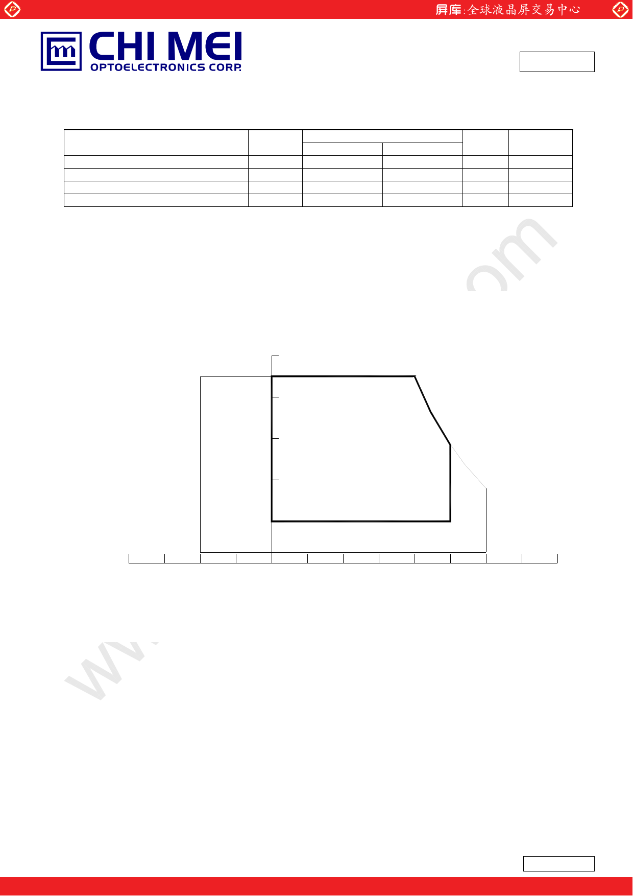
Note (1) Temperature and relative humidity range is shown in the figure below.
(a) 90 %RH Max. (Ta Љ 40 ºC).
(b) Wet-bulb temperature should be 39 ºC Max. (Ta > 40 ºC).
(c) No condensation..
Relative Humidity (%RH)
100
90
80
60
Operating Range
40
20
10 Storage Range
-40 -20
0 20 40
Temperature (ºC)
60 80
Note (2) The maximum operating temperature is based on the test condition that the surface temperature
of display area is less than or equal to 65 ºC with LCD module alone in a temperature controlled
chamber. Thermal management should be considered in your product design to prevent the
surface temperature of display area from being over 65 ºC. The range of operating temperature
may degrade in case of improper thermal management in your product design.
Note (3) The rating of environment is base on LCD module. Leave LCD cell alone, this environment condition
can’t be guaranteed. Except LCD cell, the customer has to consider the ability of other parts of LCD module
and LCD module process.
-5–
Version2.0
One step solution for LCD / PDP / OLED panel application: Datasheet, inventory and accessory! www.panelook.com
5 Page 
Global LCD Panel Exchange Center
www.panelook.com
Issued Date:Nov. 10, 2009
Model No.: V315H1-P02
Approval
5. INPUT TERMINAL PIN ASSIGNMENT
5.1 TFT LCD Module Input
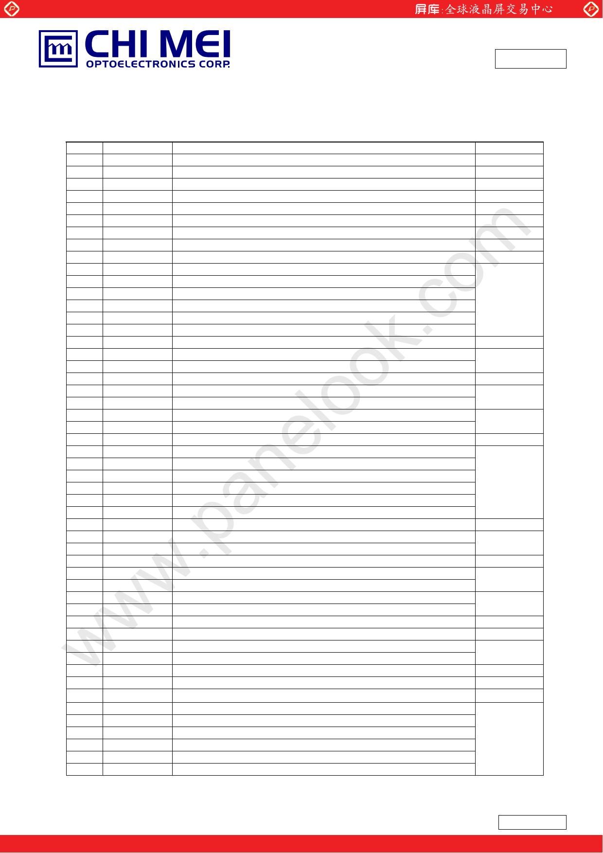
CNF1 Connector Pin Assignment
Pin Name
1 VCC
2 VCC
3 VCC
4 VCC
5 VCC
6 GND
7 GND
8 GND
9 GND
10 ORX0-
11 ORX0+
12 ORX1-
13 ORX1+
14 ORX2-
15 ORX2+
16 GND
17 OCLK-
18 OCLK+
19 GND
20 ORX3-
21 ORX3+
22 N.C.
23 N.C.
24 GND
25 ERX0-
26 ERX0+
27 ERX1-
28 ERX1+
29 ERX2-
30 ERX2+
31 GND
32 ECLK-
33 ECLK+
34 GND
35 ERX3-
36 ERX3+
37 N.C.
38 N.C.
39 GND
40 SCL
41 N.C.
42 N.C.
43 WP
44 SDA
45 LVDS_SEL
46 N.C.
47 N.C.
48 N.C.
49 N.C.
50 N.C.
51 N.C.
Description
+12V power supply
+12V power supply
+12V power supply
+12V power supply
+12V power supply
Ground
Ground
Ground
Ground
Odd pixel Negative LVDS differential data input. Channel 0
Odd pixel Positive LVDS differential data input. Channel 0
Odd pixel Negative LVDS differential data input. Channel 1
Odd pixel Positive LVDS differential data input. Channel 1
Odd pixel Negative LVDS differential data input. Channel 2
Odd pixel Positive LVDS differential data input. Channel 2
Ground
Odd pixel Negative LVDS differential clock input
Odd pixel Positive LVDS differential clock input.
Ground
Odd pixel Negative LVDS differential data input. Channel 3
Odd pixel Positive LVDS differential data input. Channel 3
No Connection
No Connection
Ground
Even pixel Negative LVDS differential data input. Channel 0
Even pixel Positive LVDS differential data input. Channel 0
Even pixel Negative LVDS differential data input. Channel 1
Even pixel Positive LVDS differential data input. Channel 1
Even pixel Negative LVDS differential data input. Channel 2
Even pixel Positive LVDS differential data input. Channel 2
Ground
Even pixel Negative LVDS differential clock input.
Even pixel Positive LVDS differential clock input.
Ground
Even pixel Negative LVDS differential data input. Channel 3
Even pixel Positive LVDS differential data input. Channel 3
No Connection
No Connection
Ground
EEPROM Serial Clock
No Connection
No Connection
EEPROM Write Protection
EEPROM Serial Data
High(3.3V) or open for VESA, Low (GND) for JEIDA
No Connection
No Connection
No Connection
No Connection
No Connection
No Connection
Note
(1)
(1)
(1)
(3)
(1)
(1)
(1)
(3)
(3)
(4)
(3)
- 11 –
Version2.0
One step solution for LCD / PDP / OLED panel application: Datasheet, inventory and accessory! www.panelook.com
11 Page | ||
| Páginas | Total 29 Páginas | |
| PDF Descargar | [ Datasheet V315H1-P02.PDF ] | |
Hoja de datos destacado
| Número de pieza | Descripción | Fabricantes |
| V315H1-P02 | TFT LCD Module | CHI MEI |
| Número de pieza | Descripción | Fabricantes |
| SLA6805M | High Voltage 3 phase Motor Driver IC. |
Sanken |
| SDC1742 | 12- and 14-Bit Hybrid Synchro / Resolver-to-Digital Converters. |
Analog Devices |
|
DataSheet.es es una pagina web que funciona como un repositorio de manuales o hoja de datos de muchos de los productos más populares, |
| DataSheet.es | 2020 | Privacy Policy | Contacto | Buscar |
