|
|
|
PDF LTC7860 Data sheet ( Hoja de datos )
| Número de pieza | LTC7860 | |
| Descripción | High Efficiency Switching Surge Stopper | |
| Fabricantes | Linear Technology | |
| Logotipo | ||
Hay una vista previa y un enlace de descarga de LTC7860 (archivo pdf) en la parte inferior de esta página. Total 26 Páginas | ||
|
No Preview Available !
LTC7860
High Efficiency Switching
Surge Stopper
Features
nn High Efficiency VOUT Clamp Stops High Voltage
Input Surges
nn SWITCH-ON Mode 100% Duty Cycle for Normal Operation
nn PROTECTIVE PWM Mode for Transients and Faults
nn
nn
VIN Pin to SGND Range: 3.5V to 60V
External Input Voltage is Extendable
to
200V+
nn Adjustable Output Voltage Clamp
nn Adjustable Output Overcurrent Protection
nn Power Inductor Improves Input EMI in Normal Operation
nn Programmable Fault Timer
nn Adjustable Soft-Start for Input Inrush Current Limiting
nn 4.5% Retry Duty Cycle During Faults
nn Adjustable Switching Frequency: 50kHz to 850kHz
nn Optional Reverse Input Voltage Protection
nn Available in Thermally Enhanced 12-lead MSOP Package
Applications
nn Industrial and Automotive Power
nn Telecom Power
nn Vehicle Power Including ISO7637
nn Military Power Including MIL1275
L, LT, LTC, LTM, OPTI-LOOP, Linear Technology, Burst Mode and the Linear logo are registered
trademarks and Hot Swap is a trademark of Linear Technology Corporation. All other trademarks
are the property of their respective owners. Protected by U.S. Patents including 5731694.
Description
The LTC®7860 high efficiency surge stopper protects loads
from high voltage transients. High efficiency permits
higher currents and smaller solution sizes. During an
input overvoltage event, such as a load dump in vehicles,
the LTC7860 controls the gate of an external MOSFET to
act as a switching DC/DC regulator (PROTECTIVE PWM
mode). This operation regulates the output voltage to a
safe level, allowing the loads to operate through the input
over-voltage event. During normal operation (SWITCH-
ON mode), the LTC7860 turns on the external MOSFET
continuously, passing the input voltage through to the
output. An internal comparator limits the voltage across
the current sense resistor and regulates the maximum
output current to protect against overcurrent faults.
An adjustable timer limits the time that the LTC7860 can
spend in overvoltage or overcurrent regulation. When the
timer expires, the external MOSFET is turned off until the
LTC7860 restarts after a cool down period. By strictly
limiting the time in PROTECTIVE PWM Mode when the
power loss is high, the components and thermal design
can be optimized for normal operation and safely oper-
ate through high voltage input surges and/or overcurrent
faults. An additional PMOS can be added for reverse
battery protection.
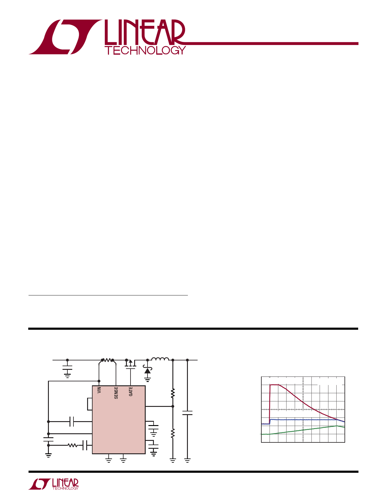
Typical Application
VIN
60V MAX
12V NOM
3.5V MIN
10µF
12mΩ
6.8µH
VOUT
18V MAX
12V NOM
3.5V MIN
5A
PROTECTIVE PWM: VOUT Clamped
to 18V During a VIN Surge
60V INPUT SURGE
CTMR = 22µF
0.47µF
VFBN
FREQ
CAP
VFB
LTC7860 TMR
0.1µF
10k 680pF RUN
ITH
SGND PGND
SS
1M
10µF
22µF
48.7k
0.1µF
7860 TA01a
VIN
10V/DIV
VOUT
10V/DIV
VTMR
1V/DIV
18V ADJUSTABLE CLAMP
100ms/DIV
7860 TA01b
7860f
For more information www.linear.com/LTC7860
1
1 page 
LTC7860
Typical Performance Characteristics TA = 25°C, unless otherwise noted.
Frequency Over Input Voltage
600
550 FREQ = OPEN
500
450
400
FREQ = 0V
350
300
0
10 20 30 40 50 60
VIN (V)
7860 G19
GATE Bias LDO (VIN - VCAP) Load
Regulation
0.5
0.0
–0.5
–1.0
–1.5
–2.0
–2.5
–3.0
–3.5
0
5 10 15
IGATE (mA)
20
7860 G22
Current Sense Voltage Over
Temperature
100
98
96
94
92
Frequency Over Temperature
600
550 FREQ = OPEN
500
450
400
FREQ = 0V
350
300
–75
–25 25
75 125
TEMPERATURE (°C)
175
7860 G20
GATE Bias LDO (VIN - VCAP)
Dropout Behavior
0.1 VIN = 5V
0.0
–0.1
–0.2
–0.3
–0.4
–0.5
0
5 10 15
IGATE (mA)
20
7860 G23
SS Pin Pull-Up Current Over
Temperature
14
VSS = 0V
12
Frequency Foldback % Over
Feedback Voltage
120
100
80
60
40
20
0
0 200 400 600 800
VFB (mV)
7860 G21
Current Sense Voltage Over ITH
Voltage
100
90
80
70
60
50
40
30
20
10
0
–10
0
0.4 0.8 1.2 1.6
ITH VOLTAGE (V)
2
7860 G24
TMR Pull-UP Current Over
Temperature
–25.0
–27.5
10 –30.0
8 –32.5
90
–75
–25 25
75 125
TEMPERATURE (°C)
175
7860 G25
6
–75 –25 25
75 125 175
TEMPERATURE (°C)
7860 G26
For more information www.linear.com/LTC7860
–35.0
–75 –50 –25
0 25 50 75 100 125 150 175
TEMPERATURE (°C)
7860 G27
7860f
5
5 Page 
Applications Information
VIN
LTC7860
VFB
Z1
VFBN
PGND SGND
FLOATING GND
QFB
RFB4
RFB3
VIN
CFB4
RFB2
VOUT
CFF
7860 F01b
RFB1
LTC7860
VIN
RFBM2
RZ2 VIN
LTC7860
QFBM2
Z1
VFBN
VFB
RFBM1
QFBM1
RFB2
Z2 RFB4
PGND SGND
QFB
FLOATING GND
RFB3 RFB1
VOUT
CFF
7860 F01c
Figure
ABOVE
1b. Switching Surge Stopper
60V with Inverting Feedback
for
VIN
Operation
translates the signal current proportional to VOUT into a
feedback voltage between VFB and VFBN. The voltage at
VFBN is the input of an inverting amplifier and is nominally
equal to the Floating Ground. The output voltage in steady
state operation is set by the feedback resistors according
to the equation:
VOUT
=
0.8V
•
RFB3
RFB4
+
VGSQFB
•
1+
RFB2
RFB1
The shunt DC bias or Zener and floating ground permits
the drain current of QFB to be translated to a differential
feedback voltage VFB – VFBN independent of the value
of VIN. RFB4 should be greater than 10k to avoid VFB pin
output current limitations.
The integrator capacitor, CFB4, should be sized to ensure
the negative sense amplifier gain rolls off and limits high
frequency gain peaking in the DC/DC control loop. The
integrator capacitor pole can be safely set to be two times
the switching frequency without affecting the DC/DC phase
margin according to the following equation. It is highly
recommended that CFB4 be used in most applications.
CFB4
=
(2
•
π
•
2
•
1
RFB4
•
FREQSW)
Great care should be taken to route the VFB and VFB lines
away from noise sources, such as the inductor or the GATE
signal that drives the external P MOSFET.
Figure 1c. Switching Surge Stopper with VIN Operation
ABOVE 60V with Non-Inverting Feedback
Non-Inverting Feedback Option
In the Non-Inverting Feedback Option for VIN ABOVE 60V,
the voltage is programmed by connecting a feedback
resistor divider from the output to ground as shown in
Figure 1c. VOUT is divided down and the voltage presented
to the base of QFB. The base voltage is then translated into
a signal current by QFB and RFB3 and sent to PNP mirror
QFBM1, RFBM1, QFBM2 and RFBM2.
In the Non-Inverting Option, the internal inverting ampli-
fier must be defeated by tying VFBN greater than 2V. In
Figure 1c, RZ2 and Z2 are used to tie VFBN high where Z2
is chosen greater than 2V but less than 6V. VFBN may also
be tied to the FREQ pin when the pin is floated and a fixed
535kHz switching frequency is selected. Choosing a fixed
535kHz in the Non-Inverting option can simplify the PCB
design and reduce component count.
For the Non-Inverting Option, an NPN is used for QFB, which
results in greater accuracy. The resistor RFB4 translates
the signal current proportional to VOUT into a feedback
voltage applied directly to the VFB pin. The VFBN pin is tied
high and the inverting amplifier is defeated. The output
voltage in steady state operation is set by the feedback
resistors according to the equation:
VOUT
=
0.8V
•
RFB3
RFB4
+
VBEQFB
•
1+
RFB2
RFB1
For more information www.linear.com/LTC7860
7860f
11
11 Page | ||
| Páginas | Total 26 Páginas | |
| PDF Descargar | [ Datasheet LTC7860.PDF ] | |
Hoja de datos destacado
| Número de pieza | Descripción | Fabricantes |
| LTC7860 | High Efficiency Switching Surge Stopper | Linear Technology |
| Número de pieza | Descripción | Fabricantes |
| SLA6805M | High Voltage 3 phase Motor Driver IC. |
Sanken |
| SDC1742 | 12- and 14-Bit Hybrid Synchro / Resolver-to-Digital Converters. |
Analog Devices |
|
DataSheet.es es una pagina web que funciona como un repositorio de manuales o hoja de datos de muchos de los productos más populares, |
| DataSheet.es | 2020 | Privacy Policy | Contacto | Buscar |