|
|
|
PDF RT9293 Data sheet ( Hoja de datos )
| Número de pieza | RT9293 | |
| Descripción | Asynchronies Boost for 10 WLED Driver | |
| Fabricantes | Richtek Technology | |
| Logotipo | ||
Hay una vista previa y un enlace de descarga de RT9293 (archivo pdf) en la parte inferior de esta página. Total 13 Páginas | ||
|
No Preview Available !
SacPower
RT9293
Small Package, High Performance, Asynchronies Boost
for 10 WLED Driver
General Description
Features
The RT9293 is a high frequency, asynchronous boost
converter. The internal MOSFET can support up to 10
White LEDs for backlighting and OLED power application,
and the internal soft start function can reduce the inrush
current. The device operates with 1-MHz fixed switching
frequency to allow small external components and to
simplify possible EMI problems. For the protection, the
RT9293A provides 50V OVP and the RT9293B provides
50V/20V OVP to allow inexpensive and small-output
capacitors with lower voltage ratings. The LED current is
initially set with the external sense resistor RSET. The
RT9293 is available in the tiny package type TSOT-23-6
and WDFN-8L 2x2 packages to provide the best solution
for PCB space saving and total BOM cost.
Ordering Information
l VIN Operating Range : 2.5V to 5.5V
l Internal Power N-MOSFET Switch
l Wide Range for PWM Dimming (100Hz to200kHz)
l Minimize the External Component Counts
l Internal Soft Start
l Internal Compensation
l Under Voltage Protection
l Over Voltage Protection
l Over Temperature Protection
l Small TSOT-23-6 and 8-Lead WDFN Packages
l RoHS Compliant and Halogen Free
Applications
l Cellular Phones
l Digital Cameras
l PDAs and Smart Phones and MP3 and OLED.
RT9293 (- )
l Portable Instruments
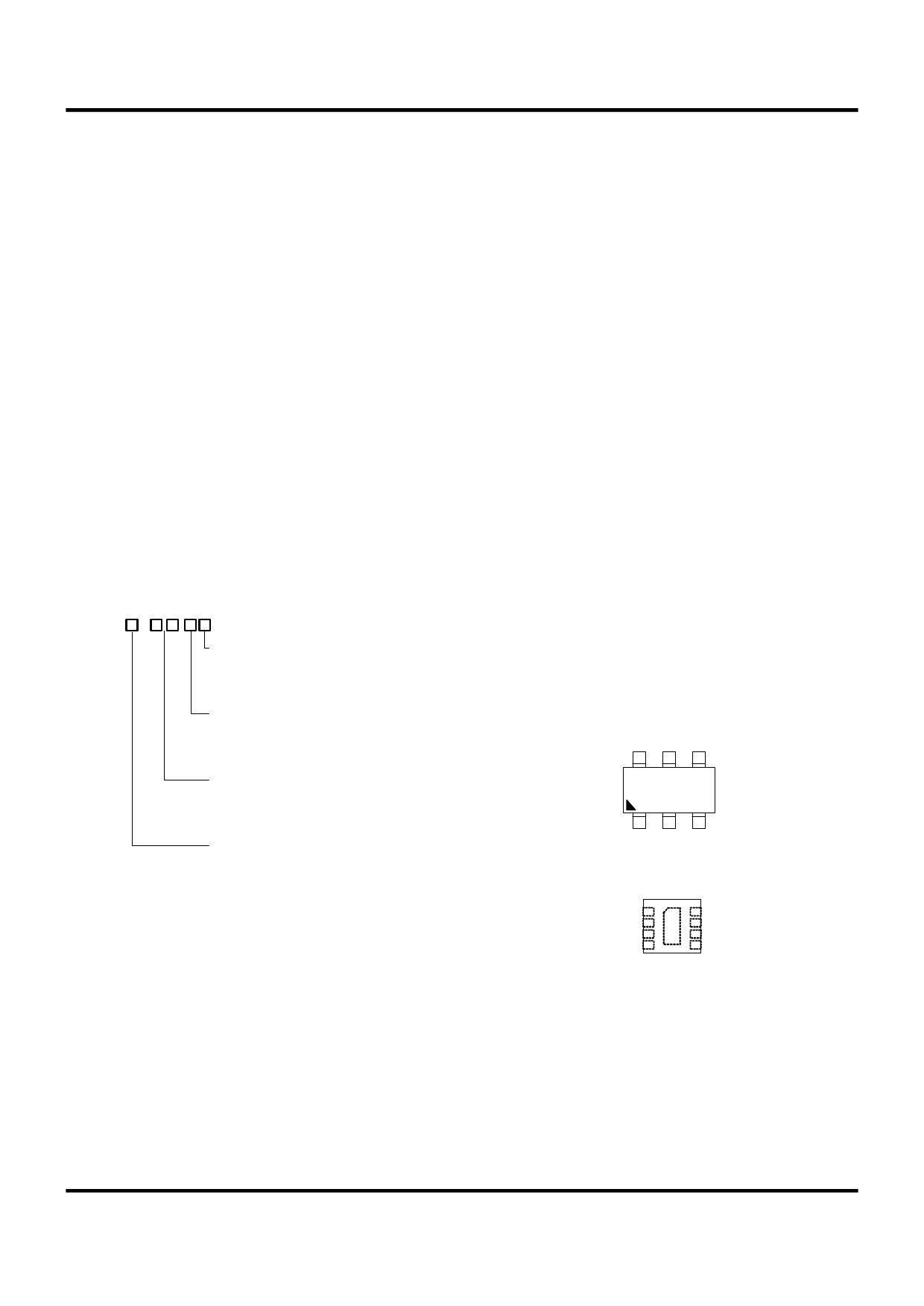
Package Type
J6 : TSOT-23-6
QW : WDFN-8L 2x2 (W-Type)
Pin Configurations
Operating Temperature Range
(TOP VIEW)
G : Green (Halogen Free with Commer-
cial Standard)
VIN VOUT EN
OVP Voltage
Default : 50V (RT9293A/B)
20 : 20V (RT9293B)
654
23
Feedback Voltage Reference
A : 104mV
B : 300mV
LX GND FB
TSOT-23-6
Note :
Richtek Green products are :
} RoHS compliant and compatible with the current require-
ments of IPC/JEDEC J-STD-020.
} Suitable for use in SnPb or Pb-free soldering processes.
GND
VIN
VOUT
EN
1
2
3
4
8 LX
7 NC
9
6 FB
5 GND
WDFN-8L 2x2
Marking Information
For marking information, contact our sales representative
directly or through a Richtek distributor located in your
area, otherwise visit our website for detail.
0755-83983280
1
1 page 
Typical Operating Characteristics
100
90
80
70
60
50
40
30
20
10
0
0
Efficiency vs. Output Current
VIN = 4.5V
VIN = 4V
VOUT = 10V
0.05 0.1 0.15 0.2 0.25 0.3
Output Current (A)
Output Voltage vs. Output Current
40
35
30
25
20
15
VIN = 3.7V, VOUT = 34V
10
5 15 25 35 45 55 65 75 85
Output Current (mA)
Frequency vs. Input Voltage
1100
1050
1000
950
900
850
ILED = 20mA
800
2.5 3 3.5 4 4.5 5 5.5
Input Voltage (V)
RT9293
100
90
80
70
60
50
40
30
20
10
0
2.5
Efficiency vs. Input Voltage
ILOAD = 30mA
ILOAD = 10mA
ILOAD = 20mA
VOUT = 34V
3 3.5 4 4.5 5 5.5
Input Voltage (V)
Quiescent Current vs. Input Voltage
500
450
400
350
300
250
VFB = 1.5V
200
2.5 3 3.5 4 4.5 5 5.5
Input Voltage (V)
Frequency vs. Temperature
1100
1050
1000
950
900
850
VIN = 3.7V, ILED = 20mA
800
-40 -25 -10 5 20 35 50 65 80 95 110 125
Temperature (°C)
5
5 Page 
RT9293
The maximum power dissipation depends on operating
ambient temperature for fixed TJ(MAX) and thermal
resistance θJA. For RT9293 packages, the Figure 7 of
derating curves allows the designer to see the effect of
rising ambient temperature on the maximum power
allowed.
0.8
0.7
WDFN-8L 2x2
0.6
Single Layer PCB
0.5
0.4
TSOT-23-6
0.3
0.2
0.1
0
0 25 50 75 100 125
Ambient Temperature (°CC)
Figure 7. Derating Curves for RT9293 Packages
The inductor should be placed as close as
possible to the switch pin to minimize the
noise coupling into other circuits.
LX node copper area should be minimized
for reducing EMI.
GND
The COUT should be connected
directly from the output schottky
diode to ground rather than
across the WLEDs
VIN
CIN should be placed
as closed as possible
to VIN pin for good
filtering.
D
L
LX
CIN
GND
RSET
FB
1
2
3
COUT
6 VIN
5 VOUT
4 EN
WLEDs
FB node copper area should be
minimized and keep far away
from noise sources (LX pin) and
RS should be as close as
possible to FB pin.
Figure 8. The Layout Consideration of the RT9293
Layout Consideration
For best performance of the RT9293, the following
guidelines must be strictly followed.
} Input and Output capacitors should be placed close to
the IC and connected to ground plane to reduce noise
coupling.
} The GND and Exposed Pad should be connected to a
strong ground plane for heat sinking and noise protection.
} Keep the main current traces as possible as short and
wide.
} LX node of DC-DC converter is with high frequency
voltage swing. It should be kept at a small area.
} Place the feedback components as close as possible
to the IC and keep away from the noisy devices.
11
11 Page | ||
| Páginas | Total 13 Páginas | |
| PDF Descargar | [ Datasheet RT9293.PDF ] | |
Hoja de datos destacado
| Número de pieza | Descripción | Fabricantes |
| RT9292 | Asyn-Boost Converter | Richtek Technology |
| RT9293 | Asynchronies Boost for 10 WLED Driver | Richtek Technology |
| RT9296 | Synchronous Boost Converter | Richtek Technology |
| RT9297 | 3A High Performance Step-Up DC/DC Converter | Richtek Technology |
| Número de pieza | Descripción | Fabricantes |
| SLA6805M | High Voltage 3 phase Motor Driver IC. |
Sanken |
| SDC1742 | 12- and 14-Bit Hybrid Synchro / Resolver-to-Digital Converters. |
Analog Devices |
|
DataSheet.es es una pagina web que funciona como un repositorio de manuales o hoja de datos de muchos de los productos más populares, |
| DataSheet.es | 2020 | Privacy Policy | Contacto | Buscar |