|
|
|
PDF ISL62882C Data sheet ( Hoja de datos )
| Número de pieza | ISL62882C | |
| Descripción | Multiphase PWM Regulator | |
| Fabricantes | Intersil Corporation | |
| Logotipo | ||
Hay una vista previa y un enlace de descarga de ISL62882C (archivo pdf) en la parte inferior de esta página. Total 30 Páginas | ||
|
No Preview Available !
Multiphase PWM Regulator for IMVP-6.5™ Mobile
CPUs and GPUs
ISL62882C
The ISL62882C is a multiphase PWM buck regulator for
miroprocessor or graphics processor core power supply.
The multiphase buck converter uses interleaved phases
to reduce the total output voltage ripple with each phase
carrying a portion of the total load current, providing
better system performance, superior thermal
management, lower component cost, reduced power
dissipation, and smaller implementation area. The
ISL62882C uses two integrated gate drivers to provide a
complete solution. The PWM modulator is based on
Intersil's Robust Ripple Regulator (R3) technology™.
Compared with traditional modulators, the R3™
modulator commands variable switching frequency
during load transients, achieving faster transient
response. With the same modulator, the switching
frequency is reduced at light load, increasing the
regulator efficiency.
The ISL62882C can be configured as CPU or graphics
Vcore controller and is fully compliant with IMVP-6.5™
specifications. It responds to PSI# and DPRSLPVR signals
by adding or dropping Phase 2, adjusting overcurrent
protection threshold accordingly, and entering/exiting
diode emulation mode. It reports the regulator output
current through the IMON pin. It senses the current by
using either discrete resistor or inductor DCR whose
variation over temperature can be thermally
compensated by a single NTC thermistor. It uses
differential remote voltage sensing to accurately regulate
the processor die voltage. The unique split LGATE
function further increases light load efficiency. The
adaptive body diode conduction time reduction function
minimizes the body diode conduction loss in diode
emulation mode. User-selectable overshoot reduction
function offers an option to aggressively reduce the
output capacitors as well as the option to disable it for
users concerned about increased system thermal stress.
The ISL62882C offers the FB2 function to optimize
1-phase performance.
Features
• Programmable 1- or 2-Phase CPU or GPU Mode
Operation
• Precision Multiphase Core Voltage Regulation
- 0.5% System Accuracy Over-Temperature
- Enhanced Load Line Accuracy
• Microprocessor Voltage Identification Input
- 7-Bit VID Input, 0V to 1.500V in 12.5mV Steps
- Supports VID Changes On-The-Fly
• Supports Multiple Current Sensing Methods
- Lossless Inductor DCR Current Sensing
- Precision Resistor Current Sensing
• Supports PSI# and DPRSLPVR modes
• Superior Noise Immunity and Transient Response
• Current Monitor and Thermal Monitor
• Differential Remote Voltage Sensing
• High Efficiency Across Entire Load Range
• Two Integrated Gate Drivers
• Excellent Dynamic Current Balance Between Phases
• Split LGATE1 Drivers Increases Light Load Efficiency
• FB2 Function Optimizes 1-Phase Mode Performance
• Adaptive Body Diode Conduction Time Reduction
• User-selectable Overshoot Reduction Function
• Small Footprint 40 Ld 5x5 TQFN Packages
• Pb-Free (RoHS Compliant)
Applications*(see page 40)
• Notebook Core Voltage Regulator
• Notebook GPU Voltage Regulator
Related Literature*(see page 40)
• See AN1461 for ISL62882/ISL62882C Evaluation Board
Application Note “ISL62882EVAL2Z User Guide”
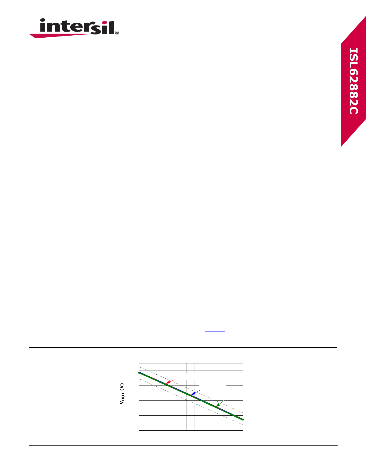
Load Line Regulation
1.10
1.08
1.06
VIN = 8V
1.04
1.02
1.00
VIN = 12V
VIN = 19V
0.98
0.96
0.94
0.92
0 5 10 15 20 25 30 35 40 45 50 55 60 65
IOUT (A)
April 29, 2010
FN7556.1
1 CAUTION: These devices are sensitive to electrostatic discharge; follow proper IC Handling Procedures.
1-888-INTERSIL or 1-888-468-3774 | Intersil (and design) is a registered trademark of Intersil Americas Inc.
Copyright © Intersil Americas Inc. 2009, 2010. All Rights Reserved
All other trademarks mentioned are the property of their respective owners.
1 page 
ISL62882C
Table of Contents
Ordering Information ......................................................................................................................... 2
Pin Configuration ................................................................................................................................ 2
Functional Pin Descriptions ................................................................................................................ 3
Block Diagram .................................................................................................................................... 6
Absolute Maximum Ratings ................................................................................................................ 7
Thermal Information .......................................................................................................................... 7
Recommended Operating Conditions .................................................................................................. 7
Electrical Specifications ...................................................................................................................... 7
Gate Driver Timing Diagram ............................................................................................................. 10
Simplified Application Circuits .......................................................................................................... 11
Theory of Operation .......................................................................................................................... 13
Multiphase R3™ Modulator ............................................................................................................... 13
Diode Emulation and Period Stretching ............................................................................................... 14
Start-up Timing .............................................................................................................................. 14
Voltage Regulation and Load Line Implementation ............................................................................... 15
Differential Sensing ......................................................................................................................... 17
Phase Current Balancing .................................................................................................................. 17
CCM Switching Frequency ................................................................................................................ 19
Modes of Operation ......................................................................................................................... 19
Dynamic Operation .......................................................................................................................... 19
Protections ..................................................................................................................................... 20
FB2 Function .................................................................................................................................. 21
Adaptive Body Diode Conduction Time Reduction ................................................................................. 21
Overshoot Reduction Function ........................................................................................................... 21
Key Component Selection ................................................................................................................. 22
RBIAS ............................................................................................................................................ 22
Inductor DCR Current-Sensing Network ............................................................................................. 22
Resistor Current-Sensing Network .................................................................................................... 24
Overcurrent Protection ..................................................................................................................... 24
Load Line Slope .............................................................................................................................. 25
Current Monitor .............................................................................................................................. 25
Compensator .................................................................................................................................. 26
Optional Slew Rate Compensation Circuit For 1-Tick VID Transition ........................................................ 28
Voltage Regulator Thermal Throttling ................................................................................................. 29
Current Balancing ........................................................................................................................... 29
Layout Guidelines ............................................................................................................................. 29
1-PHASE GPU Application Reference Design Bill of Materials ............................................................ 33
2-PHASE CPU Application Reference Design Bill of Materials ............................................................ 34
Typical Performance ......................................................................................................................... 36
Products ............................................................................................................................................ 40
Package Outline Drawing ................................................................................................................. 41
5 FN7556.1
April 29, 2010
5 Page 
ISL62882C
Simplified Application Circuits
V+5 V+5 Vin
Rbias
Rntc
oC
VDD VCCP VIN
RBIAS
NTC BOOT2
PGOOD
VR_TT#
CLK_EN#
VID<0:6>
PSI#
DPRSLPVR
VR_ON
Rdroop
PGOOD
UGATE2
VR_TT#
PHASE2
CLK_EN#
VIDs
PSI#
LGATE2
VSSP2
DPRSLPVR
ISEN2
VR_ON
VW
Rfset
BOOT1
ISL62882C
UGATE1
PHASE1
LGATE1b
COMP
FB2
FB
LGATE1a
VSSP1
ISEN1
VSEN
ISUM+
VCCSENSE
VSSSENSE
Rimon
IMON
RTN
IMON (Bottom Pad) ISUM-
VSS
Vin
L2
Rs2
Cs2
L1
Rs1
Cs1
Rn
Cn oC
Rsum2
Rsum1
Ri
Vo
FIGURE 1. TYPICAL 2-PHASE APPLICATION CIRCUIT USING DCR SENSING
V+5 V+5 Vin
Rbias
Rntc
oC
VDD VCCP VIN
RBIAS
NTC
BOOT2
IMVP6_PWRGD
VR_TT#
CLK_ENABLE
VID<0:6>#
PSI#
DPRSLPVR
VR_ON
Rdroop
PGOOD
UGATE2
VR_TT#
PHASE2
CLK_EN#
VIDs
PSI#
LGATE2
VSSP2
DPRSLPVR
ISEN2
VR_ON
VW
Rfset
BOOT1
ISL62882C
UGATE1
PHASE1
LGATE1b
COMP
FB2
FB
LGATE1a
VSSP1
ISEN1
VSEN
ISUM+
VCCSENSE
VSSSENSE
Rimon
IMON
RTN
IMON (Bottom Pad) ISUM-
VSS
Vin
L2
Rs2
Cs2
L1
Rs1
Cs1
Rsum2
Cn Rsum1
Ri
Rsen2
Vo
Rsen1
FIGURE 2. TYPICAL 2-PHASE APPLICATION CIRCUIT USING RESISTOR SENSING
11
FN7556.1
April 29, 2010
11 Page | ||
| Páginas | Total 30 Páginas | |
| PDF Descargar | [ Datasheet ISL62882C.PDF ] | |
Hoja de datos destacado
| Número de pieza | Descripción | Fabricantes |
| ISL62882 | Multiphase PWM Regulator | Intersil Corporation |
| ISL62882B | Multiphase PWM Regulator | Intersil Corporation |
| ISL62882C | Multiphase PWM Regulator | Intersil Corporation |
| Número de pieza | Descripción | Fabricantes |
| SLA6805M | High Voltage 3 phase Motor Driver IC. |
Sanken |
| SDC1742 | 12- and 14-Bit Hybrid Synchro / Resolver-to-Digital Converters. |
Analog Devices |
|
DataSheet.es es una pagina web que funciona como un repositorio de manuales o hoja de datos de muchos de los productos más populares, |
| DataSheet.es | 2020 | Privacy Policy | Contacto | Buscar |