|
|
|
PDF FTP02N60C Data sheet ( Hoja de datos )
| Número de pieza | FTP02N60C | |
| Descripción | N-Channel MOSFET | |
| Fabricantes | IPS | |
| Logotipo | ||
Hay una vista previa y un enlace de descarga de FTP02N60C (archivo pdf) en la parte inferior de esta página. Total 9 Páginas | ||
|
No Preview Available !
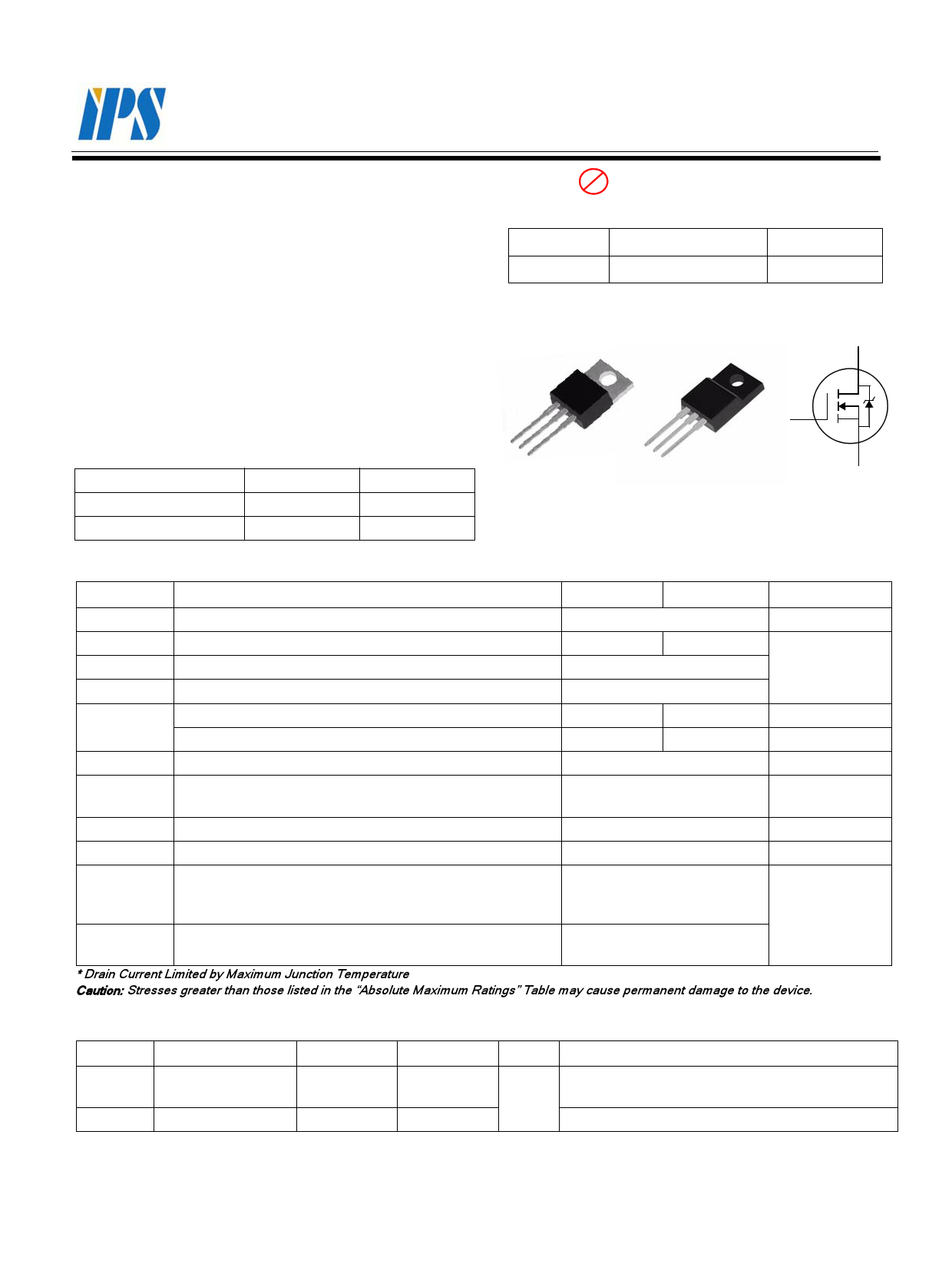
FTP02N60C
FTA02N60C
N-Channel MOSFET
Pb Lead Free Package and Finish
Applications:
• Adaptor
• TV Main Power
• SMPS Power Supply
• LCD Panel Power
Features:
• RoHS Compliant
• Low ON Resistance
• Low Gate Charge
• Peak Current vs Pulse Width Curve
Ordering Information
PART NUMBER
FTP02N60C
FTA02N60C
PACKAGE
TO-220
TO-220F
BRAND
FTP02N60C
FTA02N60C
VDSS
600 V
RDS(ON) (Max.)
4.4Ω
ID
2A
D
GDS
TO-220 G DS
TO-220F
Packages
Not to Scale
G
S
Absolute Maximum Ratings TC=25 oC unless otherwise specified
Symbol
Parameter
FTP02N60C FTA02N60C
Units
VDSS
ID
ID@ 100 oC
IDM
PD
Drain-to-Source Voltage
Continuous Drain Current
Continuous Drain Current
Pulsed Drain Current, VGS@ 10V
Power Dissipation
Derating Factor above 25 oC
(NOTE *1)
(NOTE *2)
600
2.0 2.0*
Figure 3
Figure 6
70 22
0.37 0.19
V
A
W
W/ oC
VGS
EAS
IAS
dv/dt
Gate-to-Source Voltage
Single Pulse Avalanche Engergy
L=10 mH, ID=2.67 Amps
Pulsed Avalanche Rating
Peak Diode Recovery dv/dt
(NOTE *3)
± 30
23
Figure 8
3.0
V
mJ
A
V/ ns
TL
TPKG
TJ and TSTG
Maximum Temperature for Soldering
Leads at 0.063 in (1.6 mm) from Case for 10 seconds
Package Body for 10 seconds
Operating Junction and Storage
Temperature Range
300
260
-55 to 150
oC
* Drain Current Limited by Maximum Junction Temperature
Caution: Stresses greater than those listed in the “Absolute Maximum Ratings” Table may cause permanent damage to the device.
Thermal Resistance
Symbol
Parameter
RθJC
RθJA
Junction-to-Case
Junction-to-Ambient
FTP02N60C FTA02N60C
1.78 5.6
62 100
Units
oC/W
Test Conditions
Drain lead soldered to water cooled heatsink, PD ad-
justed for a peak junction temperature of +150 oC.
1 cubic foot chamber, free air.
©2007 InPower Semiconductor Co., Ltd.
Page 1 of 9
FTP02N60C/FTA10N60C REV. A. Oct. 2007
1 page 
Figure 6. Maximum Peak Current Capability
100
TRANSCONDUCTANCE
FOR TEMPERATURES
MAY LIMIT CURRENT IN
THIS REGION
ABOVE 25oC DERATE PEAK
CURRENT AS FOLLOWS:
I = I25
-1---5---0----–-----T---C---
125
10
VGS = 10V
1
10E-6
100E-6
1E-3
10E-3
tp, Pulse Width (s)
100E-3
1E+0
10E+0
Figure 7. Typical Transfer Characteristics
5
PULSE DURATION = 380 µs
DUTY CYCLE = 0.5% MAX
4 VDS = 30 V
3
2
1
0
3
+150 oC
+25 oC
-55 oC
4 56
VGS, Gate-to-Source Voltage (V)
7
Figure 8. Unclamped Inductive
Switching Capability
100
10 STARTING TJ = 25 oC
STARTING TJ = 150 oC
1
If R= 0: tAV= (L×IAS)/(1.3BVDSS-VDD)
If R≠ 0: tAV= (L/R) ln[IAS×R)/(1.3BVDSS-VDD)+1]
R equals total Series resistance of Drain circuit
0.1
1E-6
10E-6
100E-6
1E-3
tAV, Time in Avalanche (s)
10E-3
Figure 9. Typical Drain-to-Source ON
Resistance vs Drain Current
10.5
9.0
PULSE DURATION = 10 µs
DUTY CYCLE = 0.5% MAX
TC=25°C
7.5
6.0
VGS = 10V
4.5
3.0
1.5
0
12 3 4 5
ID, Drain Current (A)
6
Figure 10. Typical Drain-to-Source ON Resistance
vs Junction Temperature
11.9
9.90
7.90
5.90
3.90
PULSE DURATION = 10 µs
DUTY CYCLE = 0.5% MAX
VGS = 10V, ID = 2.0A
1.90
-75 -50 -25 0 25 50 75 100 125 150
TJ, Junction Temperature (oC)
©2007 InPower Semiconductor Co., Ltd.
Page 5 of 9
FTP02N60C/FTA10N60C REV. A. Oct. 2007
5 Page | ||
| Páginas | Total 9 Páginas | |
| PDF Descargar | [ Datasheet FTP02N60C.PDF ] | |
Hoja de datos destacado
| Número de pieza | Descripción | Fabricantes |
| FTP02N60 | 600V N-Channel MOSFET | ark |
| FTP02N60C | N-Channel MOSFET | IPS |
| Número de pieza | Descripción | Fabricantes |
| SLA6805M | High Voltage 3 phase Motor Driver IC. |
Sanken |
| SDC1742 | 12- and 14-Bit Hybrid Synchro / Resolver-to-Digital Converters. |
Analog Devices |
|
DataSheet.es es una pagina web que funciona como un repositorio de manuales o hoja de datos de muchos de los productos más populares, |
| DataSheet.es | 2020 | Privacy Policy | Contacto | Buscar |