|
|
|
PDF RT9712 Data sheet ( Hoja de datos )
| Número de pieza | RT9712 | |
| Descripción | 1A/1.5A High-Side Dual Power Switches | |
| Fabricantes | Richtek Technology Corporation | |
| Logotipo | ||
Hay una vista previa y un enlace de descarga de RT9712 (archivo pdf) en la parte inferior de esta página. Total 14 Páginas | ||
|
No Preview Available !
®
RT9712
90mΩ, 1A/1.5A High-Side Dual Power Switches with Flag
General Description
The RT9712 power-distribution switches are designed to
fulfill the applications in heavy capacitive loads and short-
circuit situations. The device incorporates two 90mΩ N-
MOSFET power switches to fit power distribution systems
requiring multiple power switches in a single package.
During switching process, an internal charge pump is
designed to provide the gate drive for the purpose of power-
switch rise times and fall times controlling to minimize
the current surges. The charge pump can operate in supply
voltage as low as 2.7V and needs no external
components.
If the output load exceeds the current-limit threshold or a
short-circuit occurs.The RT9712 series pull the overcurrent
(FLGx) logic output low by switching into the constant-
current mode to maintain the output current in a safe level,
A thermal protection circuit turns off the switch to prevent
the device from damage when power dissipation is
increased by continuous heavy overloads and short-circuits
in the switch and finally cause the rise of the junction
temperature. The device automatically recovers when it
has sufficiently cooled down. The RT9712A/B are designed
for the current limit at typically 2A and RT9712C/D are
designed for the current limit at typically 1.5A. Internal
circuitry controls the switch to remain off until valid input
voltage is presented.
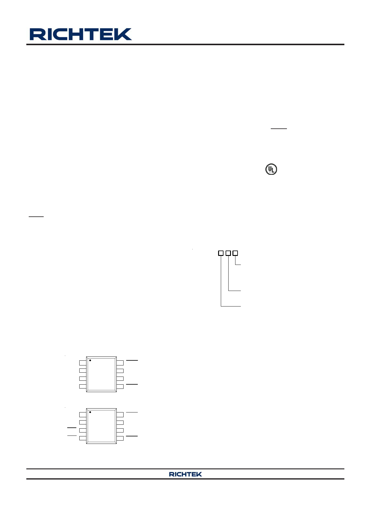
Pin Configurations
(TOP VIEW)
GND
VIN
EN1
EN2
2
3
4
8 FLG1
7 VOUT1
6 VOUT2
5 FLG2
RT9712A/C
GND
VIN
EN1
EN2
2
3
4
8 FLG1
7 VOUT1
6 VOUT2
5 FLG2
RT9712B/D
SOP-8/MSOP-8
Copyright ©2012 Richtek Technology Corporation. All rights reserved.
DS9712-04 November 2012
Features
z 90mΩ N-MOSFET Switch
z Operating Voltage Range : 2.7V to 5.5V
z Reverse Blocking Current
z Under Voltage Lockout
z Deglitched Fault Report (FLGx)
z Thermal Protection with Foldback
z Over Current Protection
z Short Circuit Protection
z UL Approved−E219878
z Nemko Approved-NO49352
z RoHS Compliant and Halogen Free
Applications
z USB Peripherals
z Notebook PCs
Ordering Information
RT9712
Package Type
S : SOP-8
F : MSOP-8
Note :
Lead Plating System
G : Green (Halogen Free and Pb Free)
Output Current/ENx Function
A : 1.5A/Active High
B : 1.5A/Active Low
C : 1A/Active High
D : 1A/Active Low
Richtek products are :
` RoHS compliant and compatible with the current require-
ments of IPC/JEDEC J-STD-020.
` Suitable for use in SnPb or Pb-free soldering processes.
Marking Information
For marking information, contact our sales representative
directly or through a Richtek distributor located in your
area.
is a registered trademark of Richtek Technology Corporation.
www.richtek.com
1
1 page 
RT9712
Parameter
Shutdown Auto-discharge
Resistance
Under Voltage Lockout
Under Voltage Hysteresis
Thermal Shutdown Protection
Thermal Shutdown Protection
Thermal Shutdown Hysteresis
Symbol
RDischarge
VUVLO
ΔVUVLO
TSD
Test Conditions
VENx = 0V, VENx = 5V
VIN Increasing
VIN Decreasing
VOUTx > 1V
VOUTx < 1V
Min Typ Max Unit
-- 100 150 Ω
1.3 1.7
-- 0.1
-- 120
-- 100
-- 20
--
--
--
--
--
V
V
°C
°C
°C
Note 1. Stresses beyond those listed “Absolute Maximum Ratings” may cause permanent damage to the device. These are
stress ratings only, and functional operation of the device at these or any other conditions beyond those indicated in the
operational sections of the specifications is not implied. Exposure to absolute maximum rating conditions may affect
device reliability.
Note 2. θJA is measured at TA = 25°C on a low effective thermal conductivity single-layer test board per JEDEC 51-3.
Note 3. Devices are ESD sensitive. Handling precaution is recommended.
Note 4. The device is not guaranteed to function outside its operating conditions.
Copyright ©2012 Richtek Technology Corporation. All rights reserved.
DS9712-04 November 2012
is a registered trademark of Richtek Technology Corporation.
www.richtek.com
5
5 Page 
RT9712
Output Filter Capacitor
A low-ESR 150μF aluminum electrolytic or tantalum
between VOUT and GND is strongly recommended to meet
the 330mV maximum droop requirement in the hub VBUS
(Per USB 2.0, output ports must have a minimum 120μF
of low-ESR bulk capacitance per hub). Standard bypass
methods should be used to minimize inductance and
resistance between the bypass capacitor and the
downstream connector to reduce EMI and decouple voltage
droop caused when downstream cables are hot-insertion
transients. Ferrite beads in series with VBUS, the ground
line and the 0.1μF bypass capacitors at the power
connector pins are recommended for EMI and ESD
protection. The bypass capacitor itself should have a low
dissipation factor to allow decoupling at higher frequencies.
Voltage Drop
The USB specification states a minimum port-output
voltage in two locations on the bus, 4.75V out of a Self-
Powered Hub port and 4.40V out of a Bus-Powered Hub
port. As with the Self-Powered Hub, all resistive voltage
drops for the Bus-Powered Hub must be accounted for to
guarantee voltage regulation (see Figure 7-47 of Universal
Serial Specification Revision 2.0 ).
The following calculation determines VOUT (MIN) for multi-
ple ports (NPORTS) ganged together through one switch (if
using one switch per port, NPORTS is equal to 1) :
VOUT (MIN) = 4.75V − [ II x ( 4 x RCONN + 2 x RCABLE ) ] −
(0.1A x NPORTS x RSWITCH ) − VPCB
Where
RCONN = Resistance of connector contacts
(two contacts per connector)
RCABLE = Resistance of upstream cable wires
(one 5V and one GND)
RSWITCH = Resistance of power switch
(90mΩ typical for RT9712A/B/C/D)
VPCB = PCB voltage drop
The USB specification defines the maximum resistance
per contact (RCONN) of the USB connector to be 30mΩ
and the drop across the PCB and switch to be 100mV.
This basically leaves two variables in the equation: the
resistance of the switch and the resistance of the cable.
If the hub consumes the maximum current (II) of 500mA,
the maximum resistance of the cable is 90mΩ.
The resistance of the switch can be defined as follows :
RSWITCH = { 4.75V − 4.4V − [ 0.5A x ( 4 x 30mΩ + 2 x
90mΩ) ] − VPCB } ÷ ( 0.1A x NPORTS )
= (200mV − VPCB ) ÷ ( 0.1A x NPORTS )
If the voltage drop across the PCB is limited to 100mV,
the maximum resistance for the switch is 250mΩ for four
ports ganged together. The RT9712A/B/C/D, with its
maximum 100mΩ on-resistance over temperature can fit
the demand of this requirement.
Thermal Shutdown
Thermal protection limits power dissipation in the
RT9712A/B/C/D. When the operation junction temperature
exceeds 120°C (typ.), the OTP circuit starts the thermal
shutdown function and turns the pass element off. The
pass element turns on again after the junction temperature
cools to 80°C. The IC lowers its OTP trip level from 120°C
to 100°C when output short circuit occurs (VOUT < 1V) as
shown in Figure 2.
VOUT Short to GND
VOUT
1V
IOUT
Thermal
Shutdown
OTP Trip
120 °C
Point
100 °C
100 °C
IC Temperature
80 °C
Figure 2. Short Circuit Thermal Folded Back Protection
when Output Short Circuit Occurs (Patent)
Copyright ©2012 Richtek Technology Corporation. All rights reserved.
DS9712-04 November 2012
is a registered trademark of Richtek Technology Corporation.
www.richtek.com
11
11 Page | ||
| Páginas | Total 14 Páginas | |
| PDF Descargar | [ Datasheet RT9712.PDF ] | |
Hoja de datos destacado
| Número de pieza | Descripción | Fabricantes |
| RT9711 | 1.5A High-Side Power Switches | Richtek Technology Corporation |
| RT9711A | 1.5A/0.6A High-Side Power Switches | Richtek Technology Corporation |
| RT9711A | 1.5A/0.6A High-Side Power Switches | Richtek |
| RT9711B | 1.5A/0.6A High-Side Power Switches | Richtek Technology Corporation |
| Número de pieza | Descripción | Fabricantes |
| SLA6805M | High Voltage 3 phase Motor Driver IC. |
Sanken |
| SDC1742 | 12- and 14-Bit Hybrid Synchro / Resolver-to-Digital Converters. |
Analog Devices |
|
DataSheet.es es una pagina web que funciona como un repositorio de manuales o hoja de datos de muchos de los productos más populares, |
| DataSheet.es | 2020 | Privacy Policy | Contacto | Buscar |