|
|
|
PDF LTC3890 Data sheet ( Hoja de datos )
| Número de pieza | LTC3890 | |
| Descripción | 2-Phase Synchronous Step-Down DC/DC Controller | |
| Fabricantes | Linear Technology | |
| Logotipo | ||
Hay una vista previa y un enlace de descarga de LTC3890 (archivo pdf) en la parte inferior de esta página. Total 30 Páginas | ||
|
No Preview Available !
FEATURES
n Wide VIN Range: 4V to 60V (65V Abs Max)
n Low Operating IQ: 50µA (One Channel On)
n Wide Output Voltage Range: 0.8V ≤ VOUT ≤ 24V
n RSENSE or DCR Current Sensing
n Out-of-Phase Controllers Reduce Required Input
Capacitance and Power Supply Induced Noise
n Phase-Lockable Frequency (75kHz to 850kHz)
n Programmable Fixed Frequency (50kHz to 900kHz)
n Selectable Continuous, Pulse-Skipping or Low Ripple
Burst Mode® Operation at Light Loads
n Selectable Current Limit
n Very Low Dropout Operation: 99% Duty Cycle
n Adjustable Output Voltage Soft-Start or Tracking
n Power Good Output Voltage Monitors
n Output Overvoltage Protection
n Low Shutdown IQ : < 14µA
n Internal LDO Powers Gate Drive from VIN or EXTVCC
n No Current Foldback During Start-Up
n Small Low Profile (0.75mm) 5mm × 5mm QFN Package
APPLICATIONS
n Automotive Always-On Systems
n Battery Operated Digital Devices
n Distributed DC Power Systems
LTC3890
60V Low IQ, Dual, 2-Phase
Synchronous Step-Down
DC/DC Controller
DESCRIPTION
The LTC®3890 is a high performance dual step-down
switching regulator DC/DC controller that drives all
N-channel synchronous power MOSFET stages. A constant
frequency current mode architecture allows a phase-
lockable frequency of up to 850kHz. Power loss and noise
due to the ESR of the input capacitor are minimized by
operating the two controller output stages out-of-phase.
The 50μA no-load quiescent current extends operating run
time in battery-powered systems. OPTI-LOOP® compensa-
tion allows the transient response to be optimized over
a wide range of output capacitance and ESR values. The
LTC3890 features a precision 0.8V reference and power
good output indicators. A wide 4V to 60V input supply
range encompasses a wide range of intermediate bus
voltages and battery chemistries.
Independent TRACK/SS pins for each controller ramp the
output voltages during start-up. Current foldback limits
MOSFET heat dissipation during short-circuit conditions.
The PLLIN/MODE pin selects among Burst Mode operation,
pulse-skipping mode, or continuous conduction mode at
light loads. For a leaded package version (28-lead Narrow
SSOP), see the LTC3890-1 data sheet.
L, LT, LTC, LTM, Burst Mode and OPTI-LOOP are registered trademarks of Linear Technology
Corporation. All other trademarks are the property of their respective owners. Protected by U.S.
Patents, including 5481178, 5705919, 5929620, 6100678, 6144194, 6177787, 6304066, 6580258,
7230497.
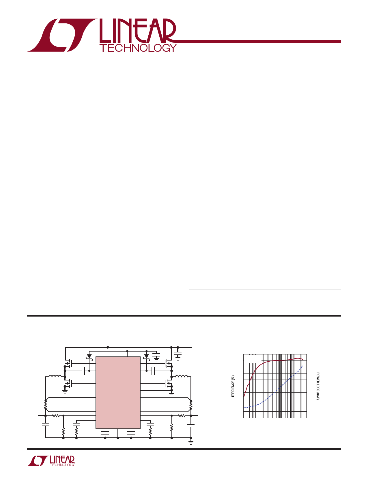
TYPICAL APPLICATION
VOUT1
3.3V
5A
High Efficiency Dual 8.5V/3.3V Output Step-Down Converter
4.7µH
0.1µF
VIN
TG1
BOOST1
SW1
INTVCC
TG2
BOOST2
SW2
4.7µF
VIN
9V TO 60V
22µF
0.1µF
8µH
BG1 BG2
LTC3890
PGND
SENSE1+
SENSE2+
0.008Ω
100k
470µF
31.6k
1000pF
SENSE1–
VFB1
ITH1
SENSE2–
VFB2
ITH2
TRACK/SS1 SGND TRACK/SS2
34.8k 0.1µF
0.1µF
1000pF
34.8k
0.01Ω
100k
10.5k
VOUT2
8.5V
3A
330µF
3890 TA01a
Efficiency and Power Loss
vs Output Current
100 VIN = 12V
90 VOUT = 3.3V
80
10000
1000
70
60 100
50
40 10
30
20 1
10
0
0.0001
0.001 0.01 0.1
1
OUTPUT CURRENT (A)
0.1
10
3890 TA01b
3890fc
1
1 page 
TYPICAL PERFORMANCE CHARACTERISTICS
LTC3890
Efficiency and Power Loss
vs Output Current
100 VIN = 12V
BURST EFFICIENCY
90 VOUT = 3.3V
80
10000
1000
70 CCM LOSS
60
100
50
40
PULSE-SKIPPING
LOSS
BURST LOSS
10
30
20
CCM EFFICIENCY
1
10
0
0.0001
PULSE-SKIPPING
EFFICIENCY
0.001 0.01 0.1
1
OUTPUT CURRENT (A)
0.1
10
FIGURE 13 CIRCUIT
3890 G01
Efficiency vs Output Current
100
90 VOUT = 8.5V
80
VOUT = 3.3V
70
60
50
40
30
20
Burst Mode OPERATION
10
0
VIN = 12V
0.0001 0.001 0.01 0.1
OUTPUT CURRENT (A)
1
FIGURE 13 CIRCUIT
10
3890 G02
Efficiency vs Input Voltage
100
98
96 VOUT2 = 8.5V
94
92
90
88 VOUT1 = 3.3V
86
84
82
80
ILOAD = 2A
0 5 10 15 20 25 30 35 40 45 50 55 60
INPUT VOLTAGE (V)
FIGURE 13 CIRCUIT
3890 G03
Load Step
Burst Mode Operation
Load Step
Pulse-Skipping Mode
Load Step
Forced Continuous Mode
VOUT
100mV/DIV
AC-
COUPLED
VOUT
100mV/DIV
AC-
COUPLED
VOUT
100mV/DIV
AC-
COUPLED
IL
2A/DIV
50µs/DIV
VIN = 12V
VOUT = 3.3V
FIGURE 13 CIRCUIT
3890 G04
IL
2A/DIV
50µs/DIV
VIN = 12V
VOUT = 3.3V
FIGURE 13 CIRCUIT
3890 G05
IL
2A/DIV
50µs/DIV
VIN = 12V
VOUT = 3.3V
FIGURE 13 CIRCUIT
3890 G06
Inductor Current at Light Load
FORCED
CONTINUOUS
MODE
Burst Mode
OPERATION
1A/DIV
PULSE-SKIPPING
MODE
VIN = 12V
VOUT = 3.3V
ILOAD = 200µA
5µs/DIV
3890 G07
Soft Start-Up
VOUT2
2V/DIV
VOUT1
2V/DIV
2ms/DIV
FIGURE 13 CIRCUIT
3890 G08
Tracking Start-Up
VOUT2
2V/DIV
VOUT1
2V/DIV
2ms/DIV
FIGURE 13 CIRCUIT
3890 G09
3890fc
5
5 Page 
LTC3890
OPERATION (Refer to the Functional Diagram)
Main Control Loop
The LTC3890 uses a constant frequency, current mode
step-down architecture with the two controller channels
operating 180 degrees out-of-phase. During normal op-
eration, each external top MOSFET is turned on when the
clock for that channel sets the RS latch, and is turned off
when the main current comparator, ICMP, resets the RS
latch. The peak inductor current at which ICMP trips and
resets the latch is controlled by the voltage on the ITH pin,
which is the output of the error amplifier, EA. The error
amplifier compares the output voltage feedback signal at
the VFB pin, (which is generated with an external resistor
divider connected across the output voltage, VOUT , to
ground) to the internal 0.800V reference voltage. When the
load current increases, it causes a slight decrease in VFB
relative to the reference, which causes the EA to increase
the ITH voltage until the average inductor current matches
the new load current.
After the top MOSFET is turned off each cycle, the bottom
MOSFET is turned on until either the inductor current starts
to reverse, as indicated by the current comparator IR, or
the beginning of the next clock cycle.
INTVCC/EXTVCC Power
Power for the top and bottom MOSFET drivers and most
other internal circuitry is derived from the INTVCC pin.
When the EXTVCC pin is tied to a voltage less than 4.7V,
the VIN LDO (low dropout linear regulator) supplies 5.1V
from VIN to INTVCC. If EXTVCC is taken above 4.7V, the VIN
LDO is turned off and an EXTVCC LDO is turned on. Once
enabled, the EXTVCC LDO supplies 5.1V from EXTVCC to
INTVCC. Using the EXTVCC pin allows the INTVCC power
to be derived from a high efficiency external source such
as one of the LTC3890 switching regulator outputs.
Each top MOSFET driver is biased from the floating boot-
strap capacitor, CB, which normally recharges during each
cycle through an external diode when the top MOSFET
turns off. If the input voltage, VIN, decreases to a voltage
close to VOUT , the loop may enter dropout and attempt
to turn on the top MOSFET continuously. The dropout
detector detects this and forces the top MOSFET off for
about one twelfth of the clock period every tenth cycle to
allow CB to recharge.
Shutdown and Start-Up (RUN1, RUN2 and
TRACK/ SS1, TRACK/SS2 Pins)
The two channels of the LTC3890 can be independently
shut down using the RUN1 and RUN2 pins. Pulling either of
these pins below 1.15V shuts down the main control loop
for that controller. Pulling both pins below 0.7V disables
both controllers and most internal circuits, including the
INTVCC LDOs. In this state, the LTC3890 draws only 14µA
of quiescent current.
Releasing either RUN pin allows a small internal current to
pull up the pin to enable that controller. The RUN1 pin has
a 7µA pull-up current while the RUN2 pin has a smaller
0.5µA. The 7µA current on RUN1 is designed to be large
enough so that the RUN1 pin can be safely floated (to
always enable the controller) without worry of condensa-
tion or other small board leakage pulling the pin down.
This is ideal for always-on applications where one or both
controllers are enabled continuously and never shut down.
The RUN pin may be externally pulled up or driven directly
by logic. When driving the RUN pin with a low impedance
source, do not exceed the absolute maximum rating of
8V. The RUN pin has an internal 11V voltage clamp that
allows the RUN pin to be connected through a resistor to a
higher voltage (for example, VIN), so long as the maximum
current into the RUN pin does not exceed 100µA.
The start-up of each controller’s output voltage VOUT is
controlled by the voltage on the TRACK/SS pin for that
channel. When the voltage on the TRACK/SS pin is less
than the 0.8V internal reference, the LTC3890 regulates
the VFB voltage to the TRACK/SS pin voltage instead of the
0.8V reference. This allows the TRACK/SS pin to be used
to program a soft-start by connecting an external capacitor
from the TRACK/SS pin to SGND. An internal 1µA pull-up
current charges this capacitor creating a voltage ramp on
the TRACK/SS pin. As the TRACK/SS voltage rises linearly
from 0V to 0.8V (and beyond up to 5V), the output voltage
VOUT rises smoothly from zero to its final value.
Alternatively the TRACK/SS pin can be used to cause the
start-up of VOUT to track that of another supply. Typically,
this requires connecting to the TRACK/SS pin an external
resistor divider from the other supply to ground (see the
Applications Information section).
3890fc
11
11 Page | ||
| Páginas | Total 30 Páginas | |
| PDF Descargar | [ Datasheet LTC3890.PDF ] | |
Hoja de datos destacado
| Número de pieza | Descripción | Fabricantes |
| LTC3890 | 2-Phase Synchronous Step-Down DC/DC Controller | Linear Technology |
| LTC3890-1 | 2-Phase Synchronous Step-Down DC/DC Controller | Linear |
| LTC3890-2 | 2-Phase Synchronous Step-Down DC/DC Controller | Linear Technology |
| LTC3890-3 | 2-Phase Synchronous Step-Down DC/DC Controller | Linear |
| Número de pieza | Descripción | Fabricantes |
| SLA6805M | High Voltage 3 phase Motor Driver IC. |
Sanken |
| SDC1742 | 12- and 14-Bit Hybrid Synchro / Resolver-to-Digital Converters. |
Analog Devices |
|
DataSheet.es es una pagina web que funciona como un repositorio de manuales o hoja de datos de muchos de los productos más populares, |
| DataSheet.es | 2020 | Privacy Policy | Contacto | Buscar |