|
|
|
PDF FDMQ8203 Data sheet ( Hoja de datos )
| Número de pieza | FDMQ8203 | |
| Descripción | Dual N-Channel and Dual P-Channel PowerTrench MOSFET | |
| Fabricantes | Fairchild Semiconductor | |
| Logotipo | ||
Hay una vista previa y un enlace de descarga de FDMQ8203 (archivo pdf) en la parte inferior de esta página. Total 10 Páginas | ||
|
No Preview Available !
FDMQ8203
December 2011
GreenBridgeTM Series of High-Efficiency Bridge Rectifiers
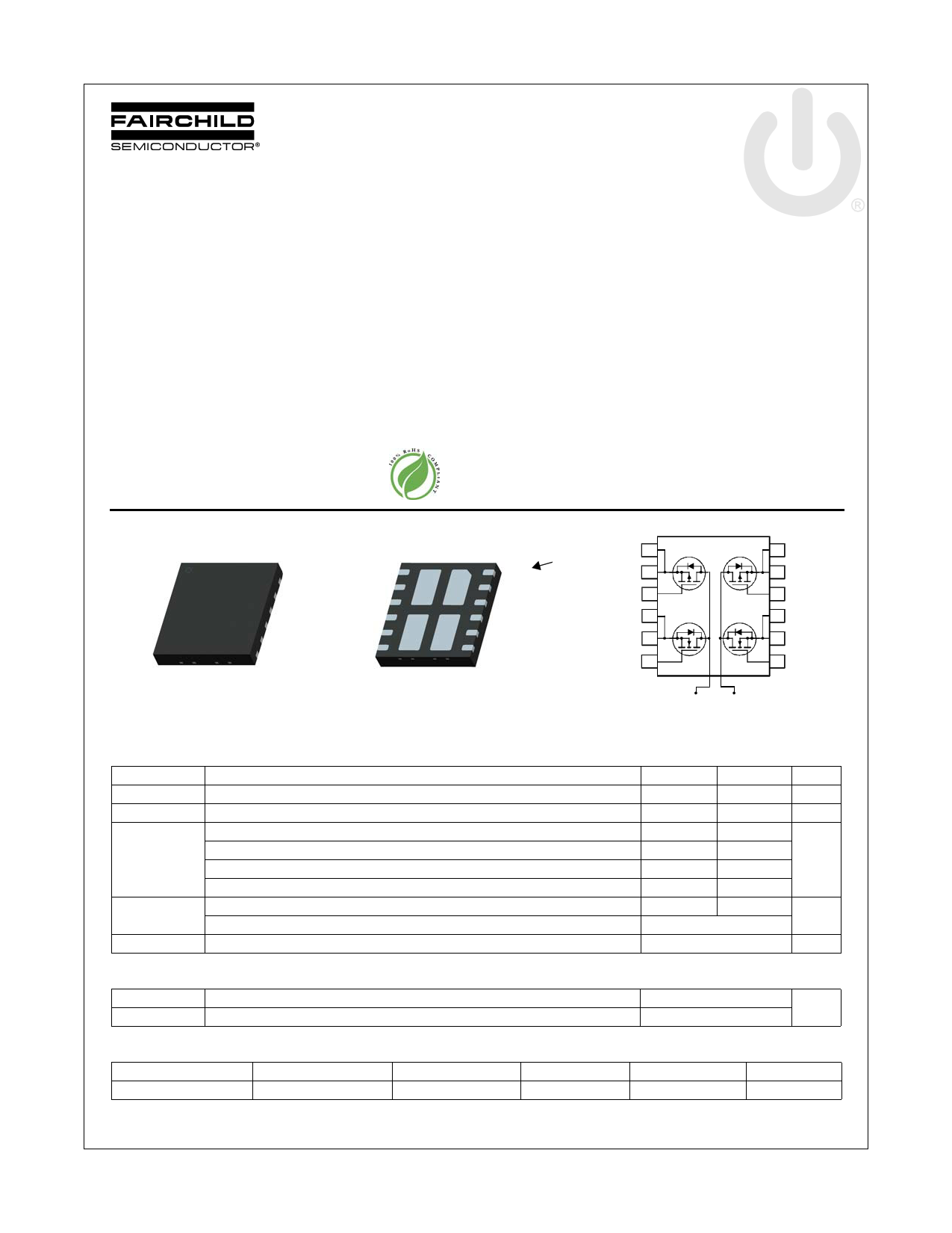
Dual N-Channel and Dual P-Channel PowerTrench® MOSFET
N-Channel: 100 V, 6 A, 110 mΩ P-Channel: -80 V, -6 A, 190 mΩ
Features
General Description
Q1/Q4: N-Channel
Max rDS(on) = 110 mΩ at VGS = 10 V, ID = 3 A
Max rDS(on) = 175 mΩ at VGS = 6 V, ID = 2.4 A
Q2/Q3: P-Channel
Max rDS(on) = 190 mΩ at VGS = -10 V, ID = -2.3 A
Max rDS(on) = 235 mΩ at VGS = -4.5 V, ID = -2.1 A
Substantial efficiency benefit in PD solutions
RoHS Compliant
This quad mosfet solution provides ten-fold improvement in
power dissipation over diode bridge.
Application
High-Efficiency Bridge Rectifiers
Top
G4
S4
S4
G3
S3
S3
Bottom
D3/ D1/
D4 D2
D3/ D1/
D4 D2
G1
S1
S1
G2
S2
S2
Pin 1
MLP 4.5x5
S3 7
S3 8
Q3 (Pch) Q2 (Pch)
6 S2
5 S2
G3 9
4 G2
S4 10
S4 11
Q4 (Nch)
Q1 (Nch)
3 S1
2 S1
G4 12
1 G1
D3,D4 to backside
(isolated from D1,D2)
D1,D2 to backside
MOSFET Maximum Ratings TA = 25 °C unless otherwise noted
Symbol
VDS
VGS
ID
PD
TJ, TSTG
Parameter
Drain to Source Voltage
Gate to Source Voltage
Drain Current
-Continuous (Package limited)
-Continuous (Silicon limited)
-Continuous
-Pulsed
TC = 25 °C
TC = 25 °C
TA = 25 °C
Power Dissipation for Single Operation
TC = 25 °C
Power Dissipation for Dual Operation
TA = 25 °C
Operating and Storage Junction Temperature Range
Thermal Characteristics
(Note 1a)
(Note 1a)
Q1/Q4
Q2/Q3
100 -80
±20 ±20
6 -6
10 -10
3.4 -2.6
12 -10
22 37
2.5
-55 to +150
Units
V
V
A
W
°C
RθJA
RθJA
Thermal Resistance, Junction to Ambient
Thermal Resistance, Junction to Ambient
Package Marking and Ordering Information
(Note 1a)
(Note 1b)
50
°C/W
160
Device Marking
FDMQ8203
Device
FDMQ8203
Package
MLP4.5x5
Reel Size
13 ”
Tape Width
12 mm
Quantity
3000 units
©2011 Fairchild Semiconductor Corporation
FDMQ8203 Rev.C1
1
www.fairchildsemi.com
1 page 
Typical Characteristics (N-Channel) TJ = 25 °C unless otherwise noted
10
ID = 3 A
8
6
VDD = 50 V
VDD = 25 V
VDD = 75 V
1000
100
Ciss
4
2
0
0 0.5 1.0 1.5 2.0 2.5 3.0
Qg, GATE CHARGE (nC)
Figure 7. Gate Charge Characteristics
20
10
Coss
10
f = 1 MHz
VGS = 0 V
1
0.1 1 10
VDS, DRAIN TO SOURCE VOLTAGE (V)
Crss
100
Figure8. Capacitance vsDrain
to Source Voltage
Figure 10.
1 ms
1
10 ms
THIS AREA IS
0.1 LIMITED BY rDS(on)
SINGLE PULSE
TJ = MAX RATED
RθJA = 160 oC/W
0.01
TA = 25 oC
0.005
0.1
1
10
100 ms
1s
10 s
DC
100 300
VDS, DRAIN to SOURCE VOLTAGE (V)
Figure 9. Forward Bias Safe Operating Area
©2011 Fairchild Semiconductor Corporation
FDMQ8203 Rev.C1
5
www.fairchildsemi.com
5 Page | ||
| Páginas | Total 10 Páginas | |
| PDF Descargar | [ Datasheet FDMQ8203.PDF ] | |
Hoja de datos destacado
| Número de pieza | Descripción | Fabricantes |
| FDMQ8203 | Dual N-Channel and Dual P-Channel PowerTrench MOSFET | Fairchild Semiconductor |
| Número de pieza | Descripción | Fabricantes |
| SLA6805M | High Voltage 3 phase Motor Driver IC. |
Sanken |
| SDC1742 | 12- and 14-Bit Hybrid Synchro / Resolver-to-Digital Converters. |
Analog Devices |
|
DataSheet.es es una pagina web que funciona como un repositorio de manuales o hoja de datos de muchos de los productos más populares, |
| DataSheet.es | 2020 | Privacy Policy | Contacto | Buscar |