|
|
|
PDF M25PX16 Data sheet ( Hoja de datos )
| Número de pieza | M25PX16 | |
| Descripción | 16-Mbit dual I/O 4-Kbyte subsector erase / serial Flash memory | |
| Fabricantes | Numonyx | |
| Logotipo | ||
Hay una vista previa y un enlace de descarga de M25PX16 (archivo pdf) en la parte inferior de esta página. Total 30 Páginas | ||
|
No Preview Available !
M25PX16
16-Mbit, dual I/O, 4-Kbyte subsector erase,
serial Flash memory with 75 MHz SPI bus interface
Features
SPI bus compatible serial interface
75 MHz (maximum) clock frequency
2.3 V to 3.6 V single supply voltage
Dual input/output instructions resulting in an
equivalent clock frequency of 150 MHz:
– Dual Output Fast Read instruction
– Dual Input Fast Program instruction
16 Mbit Flash memory
– Uniform 4-Kbyte subsectors
– Uniform 64-Kbyte sectors
Additional 64-byte user-lockable, one-time
programmable (OTP) area
Erase capability
– Subsector (4-Kbyte) granularity
– Sector (64-Kbyte) granularity
– Bulk Erase (16 Mbit) in 15 s (typical)
Write protections
– Software write protection applicable to
every 64-Kbyte sector (volatile lock bit)
– Hardware write protection: protected area
size defined by three non-volatile bits (BP0,
BP1 and BP2)
Deep Power-down mode: 5 µA (typical)
Electronic signature
– JEDEC standard two-byte signature
(7115h)
– Unique ID code (UID) with16 bytes read-
only, available upon customer request
More than 100 000 write cycles per sector
More than 20 year data retention
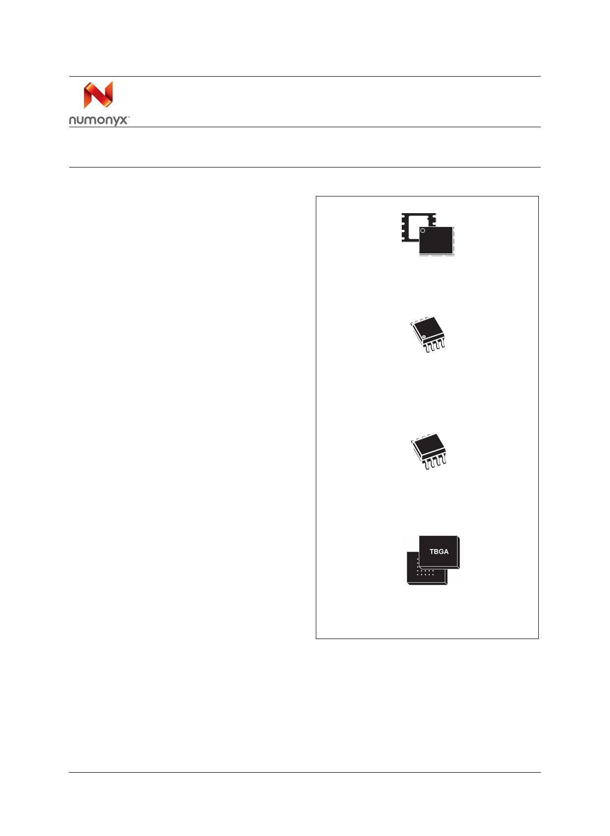
Packages
– RoHS compliant
Automotive certified parts available
VFQFPN8 (MP)
6 × 5 mm
SO8W (MW)
208 mils
SO8 (MN)
150 mils
TBGA24 (ZM) 6x8 mm
March 2010
Rev 8
1/65
www.numonyx.com
1
1 page 
M25PX16
List of figures
List of figures
Figure 1.
Figure 2.
Figure 3.
Figure 4.
Figure 5.
Figure 6.
Figure 7.
Figure 8.
Figure 9.
Figure 10.
Figure 11.
Figure 12.
Figure 13.
Figure 14.
Figure 15.
Figure 16.
Figure 17.
Figure 18.
Figure 19.
Figure 20.
Figure 21.
Figure 22.
Figure 23.
Figure 24.
Figure 25.
Figure 26.
Figure 27.
Figure 28.
Figure 29.
Figure 30.
Figure 31.
Figure 32.
Figure 33.
Figure 34.
Figure 35.
Figure 36.
Figure 37.
Figure 38.
Logic diagram . . . . . . . . . . . . . . . . . . . . . . . . . . . . . . . . . . . . . . . . . . . . . . . . . . . . . . . . . . . . 7
VFQFPN and SO8 connections . . . . . . . . . . . . . . . . . . . . . . . . . . . . . . . . . . . . . . . . . . . . . . 7
BGA 6x8 24 ball ballout . . . . . . . . . . . . . . . . . . . . . . . . . . . . . . . . . . . . . . . . . . . . . . . . . . . . 8
Bus Master and memory devices on the SPI bus . . . . . . . . . . . . . . . . . . . . . . . . . . . . . . . . 11
SPI modes supported . . . . . . . . . . . . . . . . . . . . . . . . . . . . . . . . . . . . . . . . . . . . . . . . . . . . . 12
Hold condition activation . . . . . . . . . . . . . . . . . . . . . . . . . . . . . . . . . . . . . . . . . . . . . . . . . . . 18
Block diagram . . . . . . . . . . . . . . . . . . . . . . . . . . . . . . . . . . . . . . . . . . . . . . . . . . . . . . . . . . . 19
Write Enable (WREN) instruction sequence . . . . . . . . . . . . . . . . . . . . . . . . . . . . . . . . . . . . 23
Write Disable (WRDI) instruction sequence . . . . . . . . . . . . . . . . . . . . . . . . . . . . . . . . . . . . 24
Read Identification (RDID) instruction sequence and data-out sequence . . . . . . . . . . . . . 25
Read Status Register (RDSR) instruction sequence and data-out sequence . . . . . . . . . . 27
Write Status Register (WRSR) instruction sequence . . . . . . . . . . . . . . . . . . . . . . . . . . . . . 28
Read Data Bytes (READ) instruction sequence and data-out sequence . . . . . . . . . . . . . . 30
Read Data Bytes at higher speed (FAST_READ) instruction sequence
and data-out sequence . . . . . . . . . . . . . . . . . . . . . . . . . . . . . . . . . . . . . . . . . . . . . . . . . . . . 31
Dual Output Fast Read instruction sequence . . . . . . . . . . . . . . . . . . . . . . . . . . . . . . . . . . . 32
Read Lock Register (RDLR) instruction sequence and data-out sequence . . . . . . . . . . . . 33
Read OTP (ROTP) instruction and data-out sequence . . . . . . . . . . . . . . . . . . . . . . . . . . . 34
Page Program (PP) instruction sequence . . . . . . . . . . . . . . . . . . . . . . . . . . . . . . . . . . . . . 35
Dual Input Fast Program (DIFP) instruction sequence . . . . . . . . . . . . . . . . . . . . . . . . . . . . 37
Program OTP (POTP) instruction sequence . . . . . . . . . . . . . . . . . . . . . . . . . . . . . . . . . . . 38
How to permanently lock the 64 OTP bytes . . . . . . . . . . . . . . . . . . . . . . . . . . . . . . . . . . . . 39
Write to Lock Register (WRLR) instruction sequence. . . . . . . . . . . . . . . . . . . . . . . . . . . . . 39
Subsector Erase (SSE) instruction sequence. . . . . . . . . . . . . . . . . . . . . . . . . . . . . . . . . . . 40
Sector Erase (SE) instruction sequence . . . . . . . . . . . . . . . . . . . . . . . . . . . . . . . . . . . . . . . 41
Bulk Erase (BE) instruction sequence . . . . . . . . . . . . . . . . . . . . . . . . . . . . . . . . . . . . . . . . 42
Deep Power-down (DP) instruction sequence . . . . . . . . . . . . . . . . . . . . . . . . . . . . . . . . . . 43
Release from Deep Power-down (RDP) instruction sequence . . . . . . . . . . . . . . . . . . . . . . 44
Power-up timing . . . . . . . . . . . . . . . . . . . . . . . . . . . . . . . . . . . . . . . . . . . . . . . . . . . . . . . . . 46
AC measurement I/O waveform . . . . . . . . . . . . . . . . . . . . . . . . . . . . . . . . . . . . . . . . . . . . . 49
Serial input timing . . . . . . . . . . . . . . . . . . . . . . . . . . . . . . . . . . . . . . . . . . . . . . . . . . . . . . . . 53
Write Protect Setup and Hold timing during WRSR when SRWD=1 . . . . . . . . . . . . . . . . . 53
Hold timing . . . . . . . . . . . . . . . . . . . . . . . . . . . . . . . . . . . . . . . . . . . . . . . . . . . . . . . . . . . . . 54
Output timing . . . . . . . . . . . . . . . . . . . . . . . . . . . . . . . . . . . . . . . . . . . . . . . . . . . . . . . . . . . 54
VPPH timing . . . . . . . . . . . . . . . . . . . . . . . . . . . . . . . . . . . . . . . . . . . . . . . . . . . . . . . . . . . . . 55
VFQFPN8 (MLP8) 8-lead very thin fine pitch dual flat package no lead,
6 × 5 mm, package outline . . . . . . . . . . . . . . . . . . . . . . . . . . . . . . . . . . . . . . . . . . . . . . . . . 56
SO8W 8-lead plastic small outline, 208 mils body width, package outline . . . . . . . . . . . . . 57
SO8N – 8 lead plastic small outline, 150 mils body width, package outline . . . . . . . . . . . . 58
TBGA, 6x8 mm, 24 ball package outline . . . . . . . . . . . . . . . . . . . . . . . . . . . . . . . . . . . . . . 60
5/65
5 Page 
M25PX16
3 SPI modes
SPI modes
These devices can be driven by a microcontroller with its SPI peripheral running in either of
the two following modes:
CPOL=0, CPHA=0
CPOL=1, CPHA=1
For these two modes, input data is latched in on the rising edge of Serial Clock (C), and
output data is available from the falling edge of Serial Clock (C).
The difference between the two modes, as shown in Figure 5, is the clock polarity when the
bus master is in Standby mode and not transferring data:
C remains at 0 for (CPOL=0, CPHA=0)
C remains at 1 for (CPOL=1, CPHA=1)
Figure 4. Bus Master and memory devices on the SPI bus
R
SPI interface with
(CPOL, CPHA) =
(0, 0) or (1, 1)
SDO
SDI
SCK
SPI Bus Master
VSS
VCC
C VCC
DQ1 DQ0
VSS
C VCC
DQ1 DQ0
VSS
C VCC
DQ1 DQ0
VSS
CS3 CS2 CS1
R SPI memory R
device
S W HOLD
SPI memory R
device
SPI memory
device
S
W HOLD
S
W HOLD
AI13725b
1. The Write Protect (W) and Hold (HOLD) signals should be driven, High or Low as appropriate.
Figure 4 shows an example of three devices connected to an MCU, on an SPI bus. Only
one device is selected at a time, so only one device drives the Serial Data output (DQ1) line
at a time, the other devices are high impedance. Resistors R (represented in Figure 4)
ensure that the M25PX16 is not selected if the Bus Master leaves the S line in the high
impedance state. As the Bus Master may enter a state where all inputs/outputs are in high
impedance at the same time (for example, when the Bus Master is reset), the clock line (C)
must be connected to an external pull-down resistor so that, when all inputs/outputs become
high impedance, the S line is pulled High while the C line is pulled Low (thus ensuring that S
and C do not become High at the same time, and so, that the tSHCH requirement is met).
The typical value of R is 100 kΩ, assuming that the time constant R*Cp (Cp = parasitic
capacitance of the bus line) is shorter than the time during which the Bus Master leaves the
SPI bus in high impedance.
11/65
11 Page | ||
| Páginas | Total 30 Páginas | |
| PDF Descargar | [ Datasheet M25PX16.PDF ] | |
Hoja de datos destacado
| Número de pieza | Descripción | Fabricantes |
| M25PX16 | 16-Mbit dual I/O 4-Kbyte subsector erase / serial Flash memory | Numonyx |
| M25PX16 | NOR Serial Flash Embedded Memory | Micron |
| Número de pieza | Descripción | Fabricantes |
| SLA6805M | High Voltage 3 phase Motor Driver IC. |
Sanken |
| SDC1742 | 12- and 14-Bit Hybrid Synchro / Resolver-to-Digital Converters. |
Analog Devices |
|
DataSheet.es es una pagina web que funciona como un repositorio de manuales o hoja de datos de muchos de los productos más populares, |
| DataSheet.es | 2020 | Privacy Policy | Contacto | Buscar |