|
|
PDF PZ5128 Data sheet ( Hoja de datos )
| Número de pieza | PZ5128 | |
| Descripción | 128 macrocell CPLD | |
| Fabricantes | Philips | |
| Logotipo |  |
|
Hay una vista previa y un enlace de descarga de PZ5128 (archivo pdf) en la parte inferior de esta página. Total 22 Páginas | ||
|
No Preview Available !
INTEGRATED CIRCUITS
PZ5128
128 macrocell CPLD
Product specification
Supersedes data of 1997 Apr 28
IC27 Data Handbook
Philips
Semiconductors
1997 Aug 12
1 page 
Philips Semiconductors
128 macrocell CPLD
Product specification
PZ5128
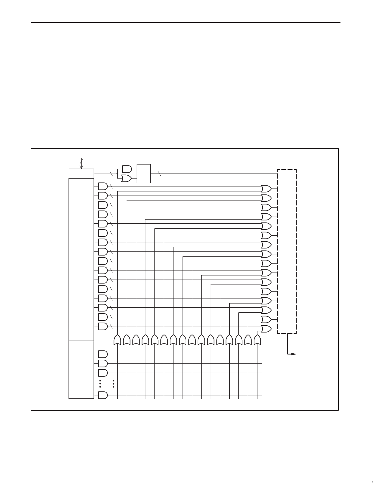
Logic Block Architecture
Figure 2 illustrates the logic block architecture. Each logic block
contains control terms, a PAL array, a PLA array, and 16 macrocells.
the 6 control terms can individually be configured as either SUM or
PRODUCT terms, and are used to control the preset/reset and
output enables of the 16 macrocells’ flip-flops. The PAL array
consists of a programmable AND array with a fixed OR array, while
the PLA array consists of a programmable AND array with a
programmable OR array. The PAL array provides a high speed path
through the array, while the PLA array provides increased product
term density.
Each macrocell has 5 dedicated product terms from the PAL array.
The pin-to-pin tPD of the PZ5128 device through the PAL array is
7.5ns. If a macrocell needs more than 5 product terms, it simply gets
the additional product terms from the PLA array. The PLA array
consists of 32 product terms, which are available for use by all 16
macrocells. The additional propagation delay incurred by a
macrocell using 1 or all 32 PLA product terms is just 2ns. So the
total pin-to-pin tPD for the PZ5128 using 6 to 37 product terms is
9.5ns (7.5ns for the PAL + 2ns for the PLA).
36 ZIA INPUTS
CONTROL
6
5
PAL
ARRAY
PLA
ARRAY
(32)
Figure 2. Philips Logic Block Architecture
1997 Aug 12
5
SP00435
5 Page 
Philips Semiconductors
128 macrocell CPLD
Product specification
PZ5128
DC ELECTRICAL CHARACTERISTICS FOR COMMERCIAL GRADE DEVICES
Commercial: 0°C ≤ Tamb ≤ +70°C; 4.75V ≤ VDD ≤ 5.25V
SYMBOL
PARAMETER
TEST CONDITIONS
MIN.
MAX.
UNIT
VIL Input voltage low
VDD = 4.75V
0.8 V
VIH Input voltage high
VDD = 5.25V
2.0
V
VI Input clamp voltage
VDD = 4.75V, IIN = –18mA
–1.2 V
VOL Output voltage low
VDD = 4.75V, IOL = 12mA
0.5 V
VOH Output voltage high
VDD = 4.75V, IOH = –12mA
2.4
V
II Input leakage current
VIN = 0 to VDD
–10 10
µA
IOZ 3-Stated output leakage current
VIN = 0 to VDD
–10 10
µA
IDDQ
Standby current
VDD = 5.25V, Tamb = 0°C
100 µA
IDDD1
Dynamic current
VDD = 5.25V, Tamb = 0°C @ 1MHz
VDD = 5.25V, Tamb = 0°C @ 50MHz
5 mA
75 mA
IOS Short circuit output current2
1 pin at a time for no longer than 1 second
–50
–200
mA
CIN
CCLK
CI/O
Input pin capacitance2
Clock input capacitance2
I/O pin capacitance2
Tamb = 25°C, f = 1MHz
Tamb = 25°C, f = 1MHz
Tamb = 25°C, f = 1MHz
8 pF
5 12 pF
10 pF
NOTES:
1. This parameter measured with a 16-bit, loadable up/down counter loaded into every logic block, with all outputs disabled and unloaded.
Inputs are tied to VDD or ground. This parameter guaranteed by design and characterization, not testing.
2. Typical values, not tested.
AC ELECTRICAL CHARACTERISTICS1 FOR COMMERCIAL GRADE DEVICES
Commercial: 0°C ≤ Tamb ≤ +70°C; 4.75V ≤ VDD ≤ 5.25V
SYMBOL
PARAMETER
–7
MIN/ MAX.
tPD_PAL Propagation delay time, input (or feedback node) to output through PAL 2 7.5
tPD_PLA
Propagation delay time, input (or feedback node) to output through PAL
& PLA
3
9.5
tCO
tSU_PAL
tSU_PLA
tH
tCH
tCL
tR
tF
fMAX1
fMAX2
fMAX3
tBUF
tPDF_PA
L
tPDF_PL
A
tCF
tINIT
tER
tEA
tRP
tRR
NOTES:
Clock to out delay time
Setup time (from input or feedback node) through PAL
Setup time (from input or feedback node) through PAL + PLA
Hold time
Clock High time
Clock Low time
Input Rise time
Input Fall time
Maximum FF toggle rate2 1/(tCH + tCL)
Maximum internal frequency2 1/(tSUPAL + tCF)
Maximum external frequency2 1/(tSUPAL + tCO)
Output buffer delay time
Input (or feedback node) to internal feedback node delay time through
PAL
Input (or feedback node) to internal feedback node delay time through
PAL+PLA
Clock to internal feedback node delay time
Delay from valid VDD to valid reset
Input to output disable3
Input to output valid
Input to register preset
Input to register reset
26
4.5
6.5
0
3
3
20
20
167
111
95
1.5
26
38
4.5
50
9
9
11
11
–10
MIN. MAX.
2 10
3 12
27
7
9
0
4
4
20
20
125
80
71
1.5
2 8.5
3 10.5
5.5
50
12
12
12.5
12.5
–12
MIN. MAX.
2 12
3 14.5
28
8
10.5
0
4
4
20
20
125
69
63
1.5
2 10.5
3 13
6.5
50
15
15
15
15
UNI
T
ns
ns
ns
ns
ns
ns
ns
ns
ns
ns
MHz
MHz
MHz
ns
ns
ns
ns
µs
ns
ns
ns
ns
1997 Aug 12
11
11 Page | ||
| Páginas | Total 22 Páginas | |
| PDF Descargar | [ Datasheet PZ5128.PDF ] | |
Hoja de datos destacado
| Número de pieza | Descripción | Fabricantes |
| PZ5128 | 128 macrocell CPLD | Philips |
| Número de pieza | Descripción | Fabricantes |
| SLA6805M | High Voltage 3 phase Motor Driver IC. |
Sanken |
| SDC1742 | 12- and 14-Bit Hybrid Synchro / Resolver-to-Digital Converters. |
Analog Devices |
|
DataSheet.es es una pagina web que funciona como un repositorio de manuales o hoja de datos de muchos de los productos más populares, |
| DataSheet.es | 2020 | Privacy Policy | Contacto | Buscar |
