|
|
|
PDF FDD26AN06A0_F085 Data sheet ( Hoja de datos )
| Número de pieza | FDD26AN06A0_F085 | |
| Descripción | N-Channel PowerTrench MOSFET | |
| Fabricantes | Fairchild Semiconductor | |
| Logotipo | ||
Hay una vista previa y un enlace de descarga de FDD26AN06A0_F085 (archivo pdf) en la parte inferior de esta página. Total 8 Páginas | ||
|
No Preview Available !
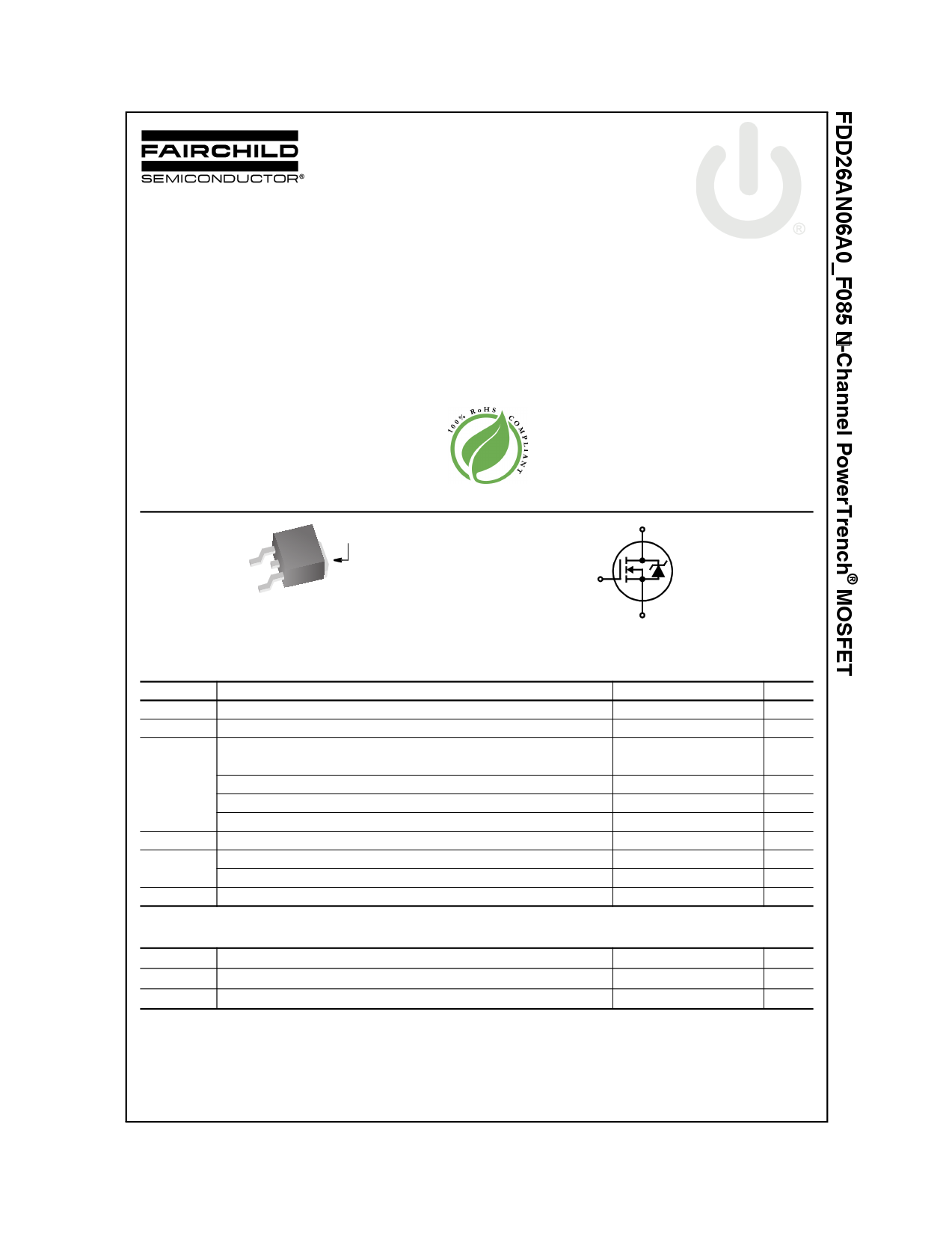
FDD26AN06A0_F085
N-Channel PowerTrench® MOSFET
60V, 36A, 26mΩ
Features
• rDS(ON) = 20mΩ (Typ.), VGS = 10V, ID = 36A
• Qg(tot) = 13nC (Typ.), VGS = 10V
• Low Miller Charge
• Low QRR Body Diode
• UIS Capability (Single Pulse and Repetitive Pulse)
• Qualified to AEC Q101
• RoHS Compliant
Aug 2011
Applications
• Motor / Body Load Control
• ABS Systems
• Powertrain Management
• Injection Systems
• DC-DC converters and Off-line UPS
• Distributed Power Architectures and VRMs
• Primary Switch for 12V and 24V systems
DRAIN
(FLANGE)
D
GATE
SOURCE
G
TO-252AA
FDD SERIES
MOSFET Maximum Ratings TC = 25°C unless otherwise noted
Symbol
VDSS
VGS
ID
EAS
PD
Parameter
Drain to Source Voltage
Gate to Source Voltage
Drain Current
Continuous (TC = 25oC, VGS = 10V)
Continuous (TC = 100oC, VGS = 10V)
Continuous (Tamb = 25oC, VGS = 10V, RθJA = 52oC/W)
Pulsed
Single Pulse Avalanche Energy ( Note 1)
Power dissipation
Derate above 25oC
TJ, TSTG Operating and Storage Temperature
S
Thermal Characteristics
RθJC
RθJA
RθJA
Thermal Resistance Junction to Case TO-252
Thermal Resistance Junction to Ambient TO-252
Thermal Resistance Junction to Ambient TO-252, 1in2 copper pad area
Ratings
60
±20
36
25
7
Figure 4
35
75
0.5
-55 to 175
2.0
100
52
Units
V
V
A
A
A
A
mJ
W
W/oC
oC
oC/W
oC/W
oC/W
This product has been designed to meet the extreme test conditions and environment demanded by the automotive industry. For a
copy of the requirements, see AEC Q101 at: http://www.aecouncil.com/
All Fairchild Semiconductor products are manufactured, assembled and tested under ISO9000 and QS9000 quality systems
certification.
©2011 Fairchild Semiconductor Corporation
FDD26AN06A0_F085 Rev. C1
1 page 
Typical Characteristics TC = 25°C unless otherwise noted
1.2 1.15
VGS = VDS, ID = 250µA
ID = 250µA
1.10
1.0
1.05
0.8
1.00
0.6
0.95
0.4
-80
-40 0 40 80 12 160
TJ, JUNCTION TEMPERATURE (oC)
200
Figure 11. Normalized Gate Threshold Voltage vs
Junction Temperature
0.90
-80
-40 0
40 80 120 160
TJ, JUNCTION TEMPERATURE (oC)
200
Figure 12. Normalized Drain to Source
Breakdown Voltage vs Junction Temperature
2000
1000
CISS = CGS + CGD
10
VDD = 30V
8
CRSS = CGD
COSS ≅ CDS + CGD
100
VGS = 0V, f = 1MHz
30
0.1 1
10
VDS, DRAIN TO SOURCE VOLTAGE (V)
60
Figure 13. Capacitance vs Drain to Source
Voltage
6
4
WAVEFORMS IN
2 DESCENDING ORDER:
ID = 36A
ID = 7A
0
0 2 4 6 8 10 12 14
Qg, GATE CHARGE (nC)
Figure 14. Gate Charge Waveforms for Constant
Gate Current
©2011 Fairchild Semiconductor Corporation
FDD26AN06A0_F085 Rev. C1
5 Page | ||
| Páginas | Total 8 Páginas | |
| PDF Descargar | [ Datasheet FDD26AN06A0_F085.PDF ] | |
Hoja de datos destacado
| Número de pieza | Descripción | Fabricantes |
| FDD26AN06A0_F085 | N-Channel PowerTrench MOSFET | Fairchild Semiconductor |
| Número de pieza | Descripción | Fabricantes |
| SLA6805M | High Voltage 3 phase Motor Driver IC. |
Sanken |
| SDC1742 | 12- and 14-Bit Hybrid Synchro / Resolver-to-Digital Converters. |
Analog Devices |
|
DataSheet.es es una pagina web que funciona como un repositorio de manuales o hoja de datos de muchos de los productos más populares, |
| DataSheet.es | 2020 | Privacy Policy | Contacto | Buscar |