|
|
|
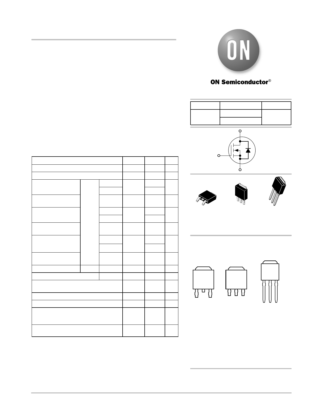
PDF NVD4809N Data sheet ( Hoja de datos )
| Número de pieza | NVD4809N | |
| Descripción | Power MOSFET ( Transistor ) | |
| Fabricantes | ON Semiconductor | |
| Logotipo | ||
Hay una vista previa y un enlace de descarga de NVD4809N (archivo pdf) en la parte inferior de esta página. Total 9 Páginas | ||
|
No Preview Available !
NTD4809N, NVD4809N
Power MOSFET
30 V, 58 A, Single N−Channel, DPAK/IPAK
Features
• Low RDS(on) to Minimize Conduction Losses
• Low Capacitance to Minimize Driver Losses
• Optimized Gate Charge to Minimize Switching Losses
• AEC Q101 Qualified − NVD4809N
• These Devices are Pb−Free and are RoHS Compliant
Applications
• CPU Power Delivery
• DC−DC Converters
• Low Side Switching
MAXIMUM RATINGS (TJ = 25°C unless otherwise noted)
Parameter
Symbol Value
Unit
Drain−to−Source Voltage
Gate−to−Source Voltage
Continuous Drain
Current (RqJA) (Note 1)
Power Dissipation
(RqJA) (Note 1)
Continuous Drain
Current (RqJA) (Note 2)
Power Dissipation
(RqJA) (Note 2)
Continuous Drain
Current (RqJC)
(Note 1)
Steady
State
TA = 25°C
TA = 85°C
TA = 25°C
TA = 25°C
TA = 85°C
TA = 25°C
TC = 25°C
TC = 85°C
VDSS
VGS
ID
PD
ID
PD
ID
30
"20
13.1
10.1
2.63
9.6
7.4
1.4
58
45
V
V
A
W
A
W
A
Power Dissipation
(RqJC) (Note 1)
TC = 25°C
Pulsed Drain Current tp=10ms TA = 25°C
Current Limited by Package
TA = 25°C
Operating Junction and Storage Temperature
PD
IDM
IDmaxPkg
TJ, Tstg
52
130
45
−55 to
175
W
A
A
°C
Source Current (Body Diode)
Drain to Source dV/dt
IS
dV/dt
43 A
6.0 V/ns
Single Pulse Drain−to−Source Avalanche
Energy (VDD = 24 V, VGS = 10 V,
L = 1.0 mH, IL(pk) = 13.5 A, RG = 25 W)
Lead Temperature for Soldering Purposes
(1/8″ from case for 10 s)
EAS 91.0 mJ
TL 260 °C
Stresses exceeding those listed in the Maximum Ratings table may damage the
device. If any of these limits are exceeded, device functionality should not be
assumed, damage may occur and reliability may be affected.
© Semiconductor Components Industries, LLC, 2014
June, 2014 − Rev. 14
1
http://onsemi.com
V(BR)DSS
30 V
RDS(on) MAX
9.0 mW @ 10 V
14 mW @ 4.5 V
D
ID MAX
58 A
N−Channel
G
S
4
4
4
12
3
DPAK
CASE 369AA
(Bent Lead)
STYLE 2
1 23
1
2
3
IPAK
IPAK
CASE 369AD CASE 369D
(Straight Lead) (Straight Lead
STYLE 2 DPAK) STYLE 2
4
Drain
MARKING DIAGRAMS
& PIN ASSIGNMENTS
4
Drain
4
Drain
2
1 Drain 3
Gate Source
1 23
Gate Drain Source
1
23
Gate Drain Source
A = Assembly Location*
Y = Year
WW = Work Week
4809N = Device Code
G = Pb−Free Package
* The Assembly Location code (A) is front side
optional. In cases where the Assembly Location is
stamped in the package, the front side assembly
code may be blank.
ORDERING INFORMATION
See detailed ordering and shipping information in the package
dimensions section on page 6 of this data sheet.
Publication Order Number:
NTD4809N/D
1 page 
NTD4809N, NVD4809N
TYPICAL PERFORMANCE CURVES
2500
2000
VDS = 0 V
Ciss
VGS = 0 V
1500
1000 Crss
TJ = 25°C
Ciss
500
Coss
0 Crss
10 5 0 5 10 15 20 25
VGS
VDS
GATE−TO−SOURCE OR DRAIN−TO−SOURCE VOLTAGE (VOLTS)
Figure 7. Capacitance Variation
1000
VDD = 15 V
ID = 30 A
VGS = 11.5 V
100
td(off)
tr
10
td(on)
tf
1
1 10 100
RG, GATE RESISTANCE (OHMS)
Figure 9. Resistive Switching Time
Variation vs. Gate Resistance
1000
100
10 ms
10
1
0.1
0.01
0.01
100 ms
VGS = 20 V
SINGLE PULSE
TA = 25°C
1 ms
10 ms
RDS(on) LIMIT
THERMAL LIMIT
PACKAGE LIMIT
dc
0.1 1 10 100
VDS, DRAIN−TO−SOURCE VOLTAGE (VOLTS)
Figure 11. Maximum Rated Forward Biased
Safe Operating Area
12
11 QT
10
9
8
7
6
5 Q1
4
Q2
3
2 ID = 30 A
1
0
0 V < VGS < 11.5 V
TJ = 25°C
0 1 2 3 4 5 6 7 8 9 1011121314151617181920212223242526
QG, TOTAL GATE CHARGE (nC)
Figure 8. Gate−To−Source and Drain−To−Source
Voltage vs. Total Charge
30
VGS = 0 V
25 TJ = 25°C
20
15
10
5
0
0.5 0.6 0.7 0.8 0.9 1.0
VSD, SOURCE−TO−DRAIN VOLTAGE (VOLTS)
Figure 10. Diode Forward Voltage vs. Current
120
ID = 15 A
100
80
60
40
20
0
25 50 75 100 125 150 175
TJ, JUNCTION TEMPERATURE (°C)
Figure 12. Maximum Avalanche Energy vs.
Starting Junction Temperature
http://onsemi.com
5
5 Page | ||
| Páginas | Total 9 Páginas | |
| PDF Descargar | [ Datasheet NVD4809N.PDF ] | |
Hoja de datos destacado
| Número de pieza | Descripción | Fabricantes |
| NVD4809N | Power MOSFET ( Transistor ) | ON Semiconductor |
| Número de pieza | Descripción | Fabricantes |
| SLA6805M | High Voltage 3 phase Motor Driver IC. |
Sanken |
| SDC1742 | 12- and 14-Bit Hybrid Synchro / Resolver-to-Digital Converters. |
Analog Devices |
|
DataSheet.es es una pagina web que funciona como un repositorio de manuales o hoja de datos de muchos de los productos más populares, |
| DataSheet.es | 2020 | Privacy Policy | Contacto | Buscar |