|
|
|
PDF LTC1699 Data sheet ( Hoja de datos )
| Número de pieza | LTC1699 | |
| Descripción | SMBus VID Voltage Programmers | |
| Fabricantes | Linear Technology | |
| Logotipo | ||
Hay una vista previa y un enlace de descarga de LTC1699 (archivo pdf) en la parte inferior de esta página. Total 20 Páginas | ||
|
No Preview Available !
LTC1699 Series
SMBus VID
Voltage Programmers
FEATURES
s Fully Compliant with Intel 5-Bit Mobile
(LTC1699-80) and Desktop VRM8.4 (LTC1699-81)
and VRM9.0 (LTC1699-82) VID Specifications
s Precision ±0.35% Programmable Resistor Divider
for Use with 0.8V Referenced DC/DC Converters
s Two Different Divider Settings Can Be Stored Using a
2-Wire SMBus Serial Interface (Rev 1.1)
s Built-In Safeguards Minimize Misprogramming Due
to Bus Conflicts
s Three Open-Drain Pins (CPU_ON, IO_ON, CLK_ON)
and a Global Control Pin (VRON)to Shutdown or
Soft-Start 3 DC/DC Converters Simultaneously
s PGOOD Pin and 50µs PGOOD Timer
s Available in MSOP-8 and SSOP-16 Package
U
APPLICATIO S
s Intel Desktop Pentium® III Power Supply
s Intel Mobile Pentium® Power Supply with Intel
SpeedStepTM Technology
s Desktop AMD AthlonTM Power Supply
s Software Programmable Remote Power Supply
s Power Supplies with Voltage Margining
DESCRIPTIO
The LTC®1699-80, LTC1699-81 and LTC1699-82 are pre-
cision (±0.35% max), digitally programmed resistor di-
viders that comply with Intel 5-bit mobile (LTC1699-80),
desktop VRM8.4 (LTC1699-81) and VRM9.0 (LTC1699-82)
VID specifications. Each IC can switch the output of a
DC/DC converter between two set voltages. A digital input
pin, SEL, selects one of two divider settings stored into
registers via a 2-wire SMBus interface.
The SMBus interface uses Write Word protocol to setup
the registers and to turn the DC/DC converters on or off.
Read Word protocol is used to verify register contents and
to return the On/Off status of the converters. The
LTC1699-80, LTC1699-81 and LTC1699-82 incorporate
safeguards against errors due to bus conflicts.
Three open-drain N-channel outputs (CPU_ON, IO_ON
and CLK_ON) are provided to turn DC/DC converter sup-
plies on or off via their RUN/SS inputs. A global control pin,
VRON is used to turn the converters on or off simulta-
neously. An internal timer pulls the PGOOD pin low for
50µs if the divider setting changes or the converters are
turned on via the SMBus and the VRON pin.
, LTC and LT are registered trademarks of Linear Technology Corporation.
AMD Athlon is a trademark of Advanced Micro Devices, Inc.
Pentium is a registered trademark of Intel Corporation.
Intel SpeedStep is a trademark of Intel Corporation.
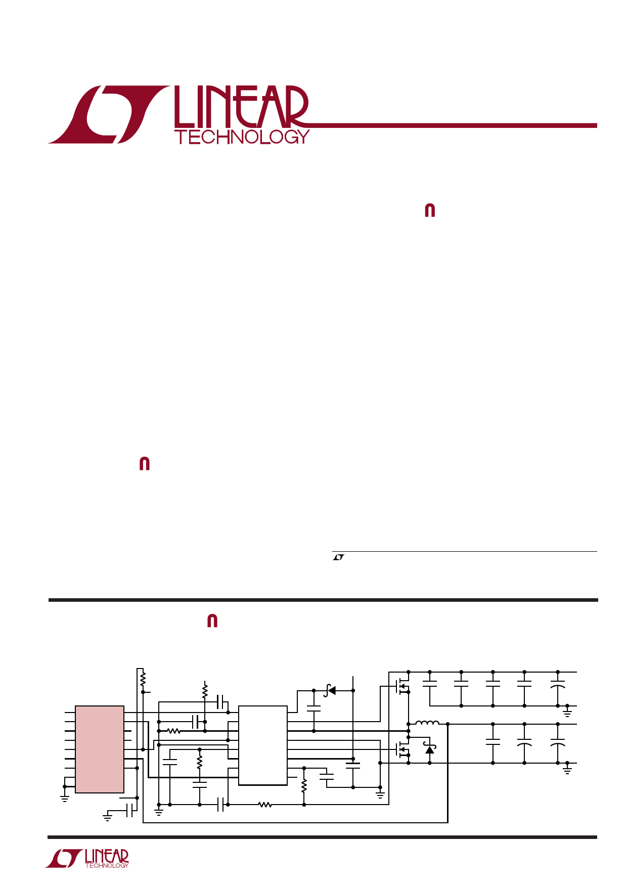
TYPICAL APPLICATIO
SMBus Controlled High Efficiency DC/DC Converter
U1
LTC1699-81
5
VRON 3 VRON
SDA 4 SDA
SCL 1 SCL
SEL 2 SEL
7 NC
11 NC
14 NC
15 GND
GND
8
CPU_ON 13
FB 9
IO_ON 10
CLK_ON 6
PGOOD 12
SENSE 16
VCC
5VDC
R9 5V
100k
PGOOD
C6
R1 0.01µF
39k
U2
LTC1778
C8, 0.01µF
R2, 11k
C15 R4
220pF 10k
C18
1 16
2 RUN/SS BOOST 15
3 PGOOD
TG 14
4 VRNG
SW 13
5 FCB
PGND 12
6 ITH
BG 11
7 SGND INTVCC 10
8 ION
VIN 9
VFB EXTVCC
2200pF
R5
715k, 1%
VIN
D1
C7
0.22µF
C13
4.7µF
C12 6.3V
R3 0.1µF
1Ω
C14, 0.1µF
C19, 0.01µF
C1 C2 C3 C4 +
M1 10µF 10µF 10µF 10µF
25V 25V 25V 25V
L1, 1µH
M2 D2
C9 +
22µF
6.3V
C10 +
180µF
4V
C1, C2, C3, C4, C9: TAIYO YUDAN
C5: SANYO
C10, C11: PANASONIC, SPCL. POLY.
D1: CMDSH-3
D2: DIODES INC., B340A
L1: TOKO, 919AS-1RON
M1: Si4884DY
M2: Si4874DY
VIN
5V
C5 TO 20V
10µF
35V
ALUM
GND
VOUT
2.5V
C11 AT 10A
180µF
4V
GND
1699 TA05
1
1 page 
LTC1699 Series
TYPICAL PERFOR A CE CHARACTERISTICS
SCL, SDA and SEL Input Current
vs Temperature
15
14 VCC = 5.5V
13 VPIN = 5.5V
12
11
10
9
8
7
6
5 SCL PIN
4
3
2
1
SEL PIN
SDA PIN
0
– 55 –35 –15 5 25 45 65 85 105 125
TEMPERATURE (°C)
1699 G09
SDA, PGOOD, CPU_ON, IO_ON,
CLK_ON Sink Current vs
Temperature
80
70
VCC = 5.5V, ISK2
60
50
40
30
20 VCC = 2.7V, ISK1
10
0
– 55 –35 –15 5 25 45 65 85 105 125
TEMPERATURE (°C)
1699 G10
PGOOD, CPU_ON, IO_ON,
CLK_ON Leakage Current vs
Temperature
7
VPIN = 5.5V
6
5
4
3
2
1
0
–60 –40 –20 0 20 40 60 80 100 120
TEMPERATURE (°C)
1699 G11
VRON Pull-Up Current vs
Temperature
2.50
2.45
2.40
2.35 VCC = 5.5V
2.30
2.25
2.20
2.15
2.10
2.05
2.00 VCC = 2.7V
1.95
1.90
– 55 –35 –15 5 25 45 65 85 105 125
TEMPERATURE (°C)
1699 G12
LTC1699-80 Divider Error vs
Temperature
0.05
VCC = 2.7V (MINIMUM VCC)
0 CODE 31
–0.05
CODE 15
CODE 16
–0.10
CODE 0
–0.15
–0.20
–55 –35 –15 5 25 45 65 85 105 125
TEMPERATURE (°C)
1699 G15
VRON Pull-Up Current vs Supply
Voltage
3.0
TA = 25°C
2.5 VRON = 0V
2.0
1.5
1.0
0.5
0
1.5 2.5 3.5 4.5 5.5 6.5
SUPPLY VOLTAGE (V)
1699 G013
LTC1699-81 Divider Error vs
Temperature
0.25
0.20 VCC = 2.7V (MINIMUM VCC)
0.15 CODE 15
0.10
0.05
0
–0.05
CODE 31
CODE 0
CODE 16
–0.10
–0.15
–0.20
–55 –35 –15 5 25 45 65 85 105 125
TEMPERATURE (°C)
1699 G16
Power Good Low Duration vs
Temperature
52.0
51.5
VCC = 5.5V
51.0
50.5
VCC = 2.7V
50.0
49.5
49.0
–60 –40 –20 0 20 40 60 80 100 120
TEMPERATURE (°C)
1699 G14
LTC1699-82 Divider Error vs
Temperature
0.16
0.14 VCC = 2.7V (MINIMUM VCC)
0.12
0.10
0.08
CODE 31
0.06
0.04
CODE 15
0.02
0 CODE 16
–0.02
CODE 0
– 55 –35 –15 5 25 45 65 85 105 125
TEMPERATURE (°C)
1699 G17
5
5 Page 
LTC1699 Series
APPLICATIO S I FOR ATIO
output voltage of a DC/DC converter that generates the
CPU core supply voltage. Its programmable ratios (see
Table 1) are designed for 0.8V-referenced converters such
as the LTC1628, LTC1702, LTC1735 and LTC1778 and
comply with the Intel 5-bit desktop (VRM8.4 for
LTC1699-81 and VRM9.0 for LTC1699-82) and 5-bit
mobile VID codes. On power-up, the outputs of both
registers are internally set to 11111B.
The LTC1699-80, LTC1699-81 and LTC1699-82 provide
three pins, CPU_ON, IO_ON, and CLK_ON to (optionally)
control three DC/DC converters that generate the CPU, I/O
and clock buffer VCC voltages in a VRM. These open drain,
N-channel output pins usually connect to the RUN/SS pins
of the converters and pull low to shut down the converters
or become a high impedance state to allow the converters
to soft-start.
The PGOOD pin is driven from an internal timer that pulls
PGOOD low for 50µs typical whenever the resistor divider
setting is changed or the converters are allowed to soft-
start. Over the entire temperature and supply voltage
range, the timer low period is 70µs max which meets the
100µs max converter output settling time specified by
Intel. The PGOOD pin, if tied to the FCB pin of an LTC DC/
DC converter, reduces the time needed for the converter
output to decrease to a lower voltage under light load
conditions by forcing the converter into continuous mode
for 50µs.
The TTL compatible VRON input pin and the output of the
internal on/off state machine (SMBON) control the state of
the CPU_ON, IO_ON, CLK_ON and PGOOD pins. SMBON
is accessed using SMBus protocols and must be pro-
grammed to a high state before the converters can turn on.
The SMBus protocols (see Figure 2) incorporate safe-
guards against errors caused by bus conflicts.
Resistor Divider
The resistor divider is designed specifically for DC/DC
converters, such as the LTC1628, LTC1702, LTC1735,
LTC1778 and LTC1929 with a reference voltage of 0.8V. It
consists of a fixed resistor, RFB1 connected between the
SENSE and FB pins and a variable resistor, RFB2, con-
nected between the FB and GND pins. The SENSE and FB
pins are tied to the output and feedback nodes of the DC/
DC converter respectively. The output of the DC/DC con-
verter is given by:
VOUT = VREF • (RFB2+RFB1)/RFB2
where VREF is the internal reference voltage of the con-
verter. Each resistor has a tolerance of ±30% but the ratio,
(RFB2+RFB1)/RFB2, is specified to within ±0.35% over
temperature. The error budget for the DC/DC converter
output voltage must include the ±0.35% ratio tolerance
and the tolerance in VREF.
The value of RFB1 is fixed and RFB2 is changed to vary the
divider setting. The value of RFB2 for any divider setting
can be calculated from the above equation, assuming that
RFB1 = 10kΩ for the LTC1699-80 and LTC1699-82 and
20kΩ for the LTC1699-81. Table 1 shows the output
voltage of a DC/DC converter (VREF = 0.8V) for all 32
settings of the resistor divider. The divider setting is
determined by the outputs (VID0-VID4) of the register
selected by the SEL pin.
SMBus Interface
The SMBus interface uses two wires: SDA and SCL. Data
to the LTC1699-80, LTC1699-81 or LTC1699-82, is latched
at the rising edge of the SCL clock input and shifted out at
the falling edge. The VIL and VIH logic threshold voltages
of the SDA and SCL pins are 0.8V and 2.1V respectively
and comply with Rev 1.1 version of the Intel System
Management Bus Specifications.
The Write Word and Read Word protocols (Figure 2) share
three common features. First, the 7-bit slave address for
both protocols is internally hardwired to 1110 001B = E2H.
A single R/W bit follows the slave address. This bit is low
for data transfer from the microprocessor to the LTC1699-
80, LTC1699-81 or LTC1699-82 and high for transfers in
the opposite direction.
Second, the LTC1699-80, LTC1699-81 and LTC1699-82
decode only the three most significant bits of the 8-bit
command code. Table 2 shows the four valid combina-
tions. All other combinations are ignored.
Third, the Data Low and Data High bytes correspond to
Registers 0 and 1 respectively. In Write Word protocol with
C7 = C6 = 0, C5 = 1, the five most significant bits (VID0-
VID4) of these bytes specify a resistor divider setting.
11
11 Page | ||
| Páginas | Total 20 Páginas | |
| PDF Descargar | [ Datasheet LTC1699.PDF ] | |
Hoja de datos destacado
| Número de pieza | Descripción | Fabricantes |
| LTC1690 | Differential Driver and Receiver Pair with Fail-Safe Receiver Output | Linear Technology |
| LTC1690C | Differential Driver and Receiver Pair with Fail-Safe Receiver Output | Linear Technology |
| LTC1690CMS8 | Differential Driver and Receiver Pair with Fail-Safe Receiver Output | Linear Technology |
| LTC1690CN8 | Differential Driver and Receiver Pair with Fail-Safe Receiver Output | Linear Technology |
| Número de pieza | Descripción | Fabricantes |
| SLA6805M | High Voltage 3 phase Motor Driver IC. |
Sanken |
| SDC1742 | 12- and 14-Bit Hybrid Synchro / Resolver-to-Digital Converters. |
Analog Devices |
|
DataSheet.es es una pagina web que funciona como un repositorio de manuales o hoja de datos de muchos de los productos más populares, |
| DataSheet.es | 2020 | Privacy Policy | Contacto | Buscar |