|
|
PDF AZ4052 Data sheet ( Hoja de datos )
| Número de pieza | AZ4052 | |
| Descripción | Dual 4-channel Analog Multiplexer/Demultiplexer | |
| Fabricantes | BCD Semiconductor | |
| Logotipo | ||
Hay una vista previa y un enlace de descarga de AZ4052 (archivo pdf) en la parte inferior de esta página. Total 18 Páginas | ||
|
No Preview Available !
Preliminary Datasheet
Dual 4-channel Analog Multiplexer/Demultiplexer
AZ4052
General Description
The AZ4052 is high-speed si-gate CMOS device. The
AZ4052 is dual 4-channel analog multiplexers or
demultiplexers with common select logic. Each
multiplexer has four independent inputs/outputs (pins
nY0 to nY3) and a common input/output (pin nZ).
The common channel select logics include two digital
select inputs (pins S0 and S1) and an active LOW
___ ___
enable input (pin E). When pin E=LOW, one of the
four switches is selected (Low-impedance On-state)
___
with pins S0 and S1. When pin E =HIGH, all
switches are in the high-impedance Off-state,
independent of pins S0 and S1. VCC and GND are the
supply voltage pins for the digital control inputs (pins
___
S0, S1 and E). The VCC to GND ranges are 3.0V to
10V. The analog inputs/outputs (pins nY0 to nY3 and
nZ) can swing between VCC as a positive limit and
VEE as a negative limit. VCC-VEE may not exceed 10V.
For operation as a digital multiplexer/demultiplexer,
VEE is connected to GND (Typically Ground).
The AZ4052 is available in standard packages of
SOIC-16 and DIP-16.
Features
• Wide Operation Voltage: ±5.0V or 10V
• Low On-resistance:
- 55Ω (Typ.) at VCC-VEE=5V
- 40Ω ( Typ.) at VCC-VEE=10V
• Ultra Low THD+N:
0.003% @ 10V, 0.008% @ 5.0V
• Ultra Low Crosstalk: -120dB
• Ultra Low Noise: 6.0μVRMS
• Operating Temperature: -40ºC to 85ºC
Applications
• LCD TV/PDP TV/CRT TV
• 4:1 Multi-channel Signal Selecting
Function Table
Control Input
___
E
S1
S0
LL
L
LL
H
LH
L
LH
H
HX
X
On Channel
nY0
nY1
nY2
nY3
None
nZ
nZ
nZ
nZ
SOIC-16
DIP-16
Figure 1. Package Types of AZ4052
Oct. 2011 Rev. 1.1
BCD Semiconductor Manufacturing Limited
1
1 page 
Preliminary Datasheet
Dual 4-channel Analog Multiplexer/Demultiplexer
AZ4052
Absolute Maximum Ratings (Note 1, 2)
Parameter
Power Supply Voltage
Input Diode Current
Symbol
VCC
IIK
Switch Diode Current
Switch Current
VEE Current
VCC Current
GND Current
Power Dissipation
Storage Temperature Range
Operating
Junction
Temperature Range
Power Dissipation Per Switch
ESD (Machine Model)
ESD (Human Body Model)
ISK
IS
IEE
ICC
IGND
PD
TSTG
TJ
PS
Condition
VI<-0.5V,
VI>VCC+0.5V
VS<-0.5V,
VS>VCC+0.5V
-0.5V<VS<VCC+0.5V
TA=-40ºC to 85ºC
(Note 3)
Value
-0.5 to 11.0
20
20
25
20
50
500
-65 to 150
150
100
200
2000
Unit
V
mA
mA
mA
mA
mA
mW
ºC
ºC
mW
V
V
Note 1: Stresses greater than those listed under “Absolute Maximum Ratings” may cause permanent damage to
the device. These are stress ratings only and functional operation of the device at these or any other conditions
beyond those indicated under “Recommended Operating Conditions” is not implied. Exposure to “Absolute
Maximum Ratings” for extended periods may affect device reliability.
Note 2: To avoid drawing VCC current out of pins nZ, when switch current flows in pins nYn, the voltage drop
across the bidirectional switch must not exceed 0.4V. If the switch current flows into pins nZ, no VCC current
will flow out of pins nYn. In this case there is no limit for the voltage drop across the switch, but the voltages at
pins nYn and nZ may not exceed VCC or VEE.
Note 3: Above 70ºC derate linearly with 12mW/K (DIP-16 package).
Above 70ºC derate linearly with 8mW/K (SOIC-16 package)
Oct. 2011 Rev. 1. 1
BCD Semiconductor Manufacturing Limited
5
5 Page 
Preliminary Datasheet
Dual 4-channel Analog Multiplexer/Demultiplexer
AZ4052
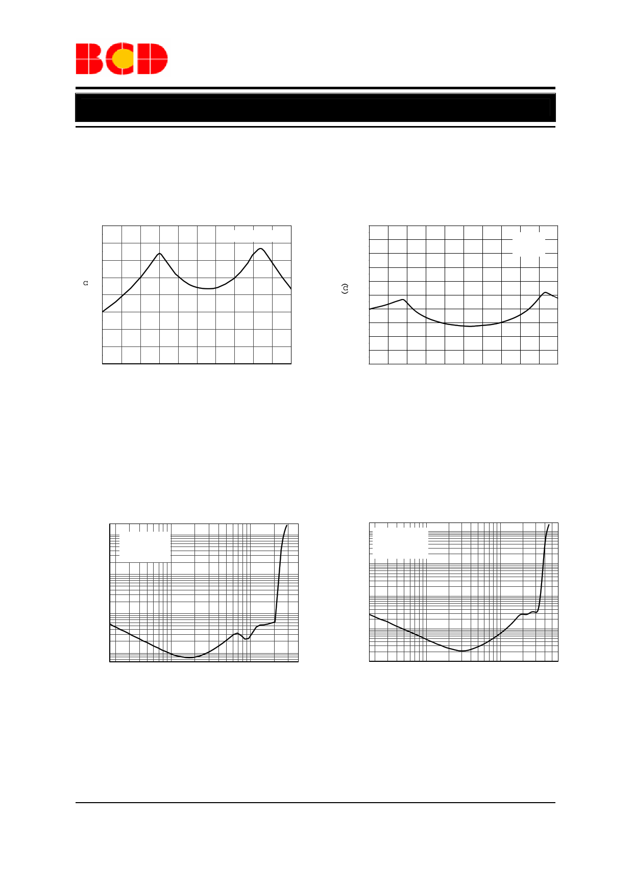
Typical Performance Characteristics
80
V =5V,V =0V
CC EE
75
70
65
60
55
50
45
40
0.0 0.5 1.0 1.5 2.0 2.5 3.0 3.5 4.0 4.5 5.0
Signal Output (V)
Figure 13. RDSON vs. Signal Output
70
65
V =10V
CC
V =0V
60 EE
55
50
45
40
35
30
25
20
0 2 4 6 8 10
Signal Output (V)
Figure 14. RDSON vs. Signal Output
10 V =5V,V =0V
CC EE
R =10kΩ
L
f=1kHz
1
0.1
0.01
0.1 1
Output Voltage Amplitude
Figure 15. THD+N vs. Output Voltage Amplitude
10 V =10V,V =0V
CC EE
R =10kΩ
L
f=1kHz
1
0.1
0.01
1E-3
0.1
1
Output Voltage Amplitude
Figure 16. THD+N vs. Output Voltage Amplitude
Oct. 2011 Rev. 1. 1
BCD Semiconductor Manufacturing Limited
11
11 Page | ||
| Páginas | Total 18 Páginas | |
| PDF Descargar | [ Datasheet AZ4052.PDF ] | |
Hoja de datos destacado
| Número de pieza | Descripción | Fabricantes |
| AZ4052 | Dual 4-channel Analog Multiplexer/Demultiplexer | BCD Semiconductor |
| Número de pieza | Descripción | Fabricantes |
| SLA6805M | High Voltage 3 phase Motor Driver IC. |
Sanken |
| SDC1742 | 12- and 14-Bit Hybrid Synchro / Resolver-to-Digital Converters. |
Analog Devices |
|
DataSheet.es es una pagina web que funciona como un repositorio de manuales o hoja de datos de muchos de los productos más populares, |
| DataSheet.es | 2020 | Privacy Policy | Contacto | Buscar |
