|
|
|
PDF AS1844 Data sheet ( Hoja de datos )
| Número de pieza | AS1844 | |
| Descripción | Digital Power PoE PD Controllers | |
| Fabricantes | Akros Silicon | |
| Logotipo | ||
Hay una vista previa y un enlace de descarga de AS1844 (archivo pdf) en la parte inferior de esta página. Total 30 Páginas | ||
|
No Preview Available !
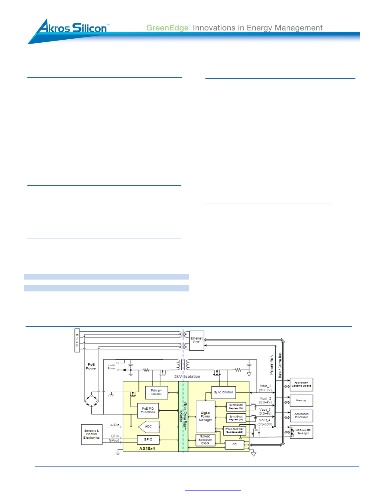
AS1854/44/34/24 — Digital Power PoE PD Controllers
with HV Isolation and Quad DC-DC Outputs
GENERAL DESCRIPTION
The AS18x4 product family integrates Akros GreenEdge™ Isolation
technology with next generation Power-over-Ethernet (PoE) PD and
power conversion technology to deliver groundbreaking power
integration, and enable a new range of Digital Power PoE PD
capabilities and solutions.
A Type 1 (IEEE® 802.3af) and Type 2 (IEEE® 802.3at) compliant PD
is integrated with high-voltage isolation and quad-output digital
power DC-DC converters – resulting in a complete PoE & Power
management solution in a single device with minimal external
components.
In addition to enabling digital PoE power conversion, Akros
GreenEdge™ isolation enables direct digital management of both
isolated Primary power and Secondary system power for real time
end-to-end Green Power application capabilities.
TYPICAL APPLICATIONS
� Voice-over-IP (VoIP) phones
� Wireless LAN & WiMAX access points (WAP)
� Pan, Tilt, Zoom (PTZ) Cameras, IP cameras
� Thin-client and notebook computers
� Fiber-to-the-home (FTTH) terminals
� Point-of-sale (PoS) terminals, RFID readers
ORDERING INFORMATION
The AS18x4 family includes four pin-compatible devices, all available
in 64-lead QFN Reduction of Hazardous Substance (RoHS)
compliant packages.
Part #
Type 1 Type 2 Hardware
PD PD Mode
AS1824*
x
x
AS1834*
x
x
AS1844*
x
x
x
AS1854*
x
x
x
* Industrial Temperature Range, -40°C to 85°C
Software
Mode
x
x
Pwr In
(W)
13
13
13/30
13/30
FEATURES
PoE PD Controller
� Type 1 and Type 2 IEEE® 802.3af & 802.3at Compliant PD
� Automatic PoE-Plus (Type 2) detection in HW and
I2C Modes
� Low Resistance PD Power FET Switch (0.5 typical)
Primary‐Side DC‐DC Controller
� High-efficiency DC-DC Controller with Digital Optimization
� Primary-Secondary High-voltage integrated Digital Isolation
� Programmable Primary Clock Frequency
� Local-power operation down to 9.5V
Secondary‐Side Power Outputs
� Programmable PWM Frequencies synched to External Clock
� Output #1: Sync Controller with programmable power FET
timing for high efficiency at both light and full load
� Outputs #2 & #3: Buck Regulators w/2A FETs
� Output #4: DC-DC Controller for Buck, Boost, or LED Boost
platform applications
EMC Compliance and Protection
� Slew-rate-controlled power drivers
� Multi-phased PWM clocking, with External Sync clock option
� Optional spread-spectrum clocking available for all PWMs
� Over-current, Under/Over-voltage and Short-circuit Protection
� High-temperature warning and shutdown
� Meets IEC 61000-4-2/3/4/5/6, IEC60747, IEC 60950, DIN
EN60747-5-2 (VDE0884), & UL1577 requirements for EMC
compliance and basic isolation to 2120 VDC (1500 VRMS)
� 100V Process for PoE transient voltage robustness
SIMPLIFIED APPLICATION DIAGRAM
Akros Silicon, Inc.
6399 San Ignacio Avenue, Suite 250, San Jose, CA 95119 USA
408.746.9000 http://www.AkrosSilicon.com
1 page 
AS1854/44/34/24
Table 16 - Typical LDET External Resistor Design ....................................................................................................................23
Table 17 - PWM Clock Rate Configuration.................................................................................................................................24
Table 18 - Sync & Overlap Delay Timing Limit...........................................................................................................................25
Table 19 - SYNC_DLY & SYNC_OVL Resistor Calculation Example ........................................................................................26
Table 20 - AS1854/34 Device Address Configuration ................................................................................................................35
Table 21 - AS1854/34 Register Address Word ..........................................................................................................................36
Table 22 - AS1854/34 Register and Bit Summary......................................................................................................................37
Table 23 - Alarms and Power Status (Read-Only) - 00h ............................................................................................................38
Table 24 - Interrupt Mask (R/W) - 01h........................................................................................................................................38
Table 25 - Interrupt Status (Read-Only) - 02h ............................................................................................................................39
Table 26 - PGOOD Voltage Masks (R/W) - 03h.........................................................................................................................39
Table 27 - Watchdog Enable, Mask, Service (R/W) - 04h ..........................................................................................................40
Table 28 - PGOOD & Watchdog History (R/W) - 05h.................................................................................................................40
Table 29 - Device Control and I/O Status (R/W) - 06h ...............................................................................................................41
Table 30 - Watchdog Timeout (R/W) - 07h.................................................................................................................................41
Table 31 - ADCIN Voltage (Read-Only) - 08h ............................................................................................................................42
Table 32 - ADCIN Alarm Threshold (R/W) - 09h ........................................................................................................................42
Table 33 - PD Status and System Clock Control (R/W) - 0Ah....................................................................................................42
Table 34 - PD Voltage (Read-Only) - 0Bh ..................................................................................................................................43
Table 35 - PD Current (Read-Only) - 0Ch ..................................................................................................................................43
Table 36 - PD Over-Current Alarm Threshold (R/W) - 0Dh ........................................................................................................44
Table 37 - Outputs 1, 2 Disable & Margin Control (R/W) - 0Eh ..................................................................................................44
Table 38 - Outputs 3, 4 Disable & Margin Control (R/W) - 0Fh ..................................................................................................45
Table 39 - PoE Design Framework Summary ............................................................................................................................46
Akros Silicon, Inc.
6399 San Ignacio Avenue, Suite 250, San Jose, CA 95119 USA
408.746.9000 http://www.AkrosSilicon.com
5
5 Page 
AS1854/44/34/24
59
INTB /
AT_DET
OD
Secondary Side: Inputs & Outputs
INTB in Software Mode. The I2C interface interrupts output, active low. The open drain
output allows user defined voltage output high level.
AT_DET in Hardware Mode. It is the PoE+ (802.3at) PSE detect indication output. A
High level output indicates connection to either a Type 2 PSE or to a Local Power
supply. The output is open drain, active High. If a Type 1 PSE is connected, the output
of AT_DET remains in the inactive state (Low).
DC coupled clock input for timing of Primary and Secondary DC-DC regulators &
60
CLK_IN
I, PU controllers if synchronizing to an external time source is desired. Nominally sourced
from the local Ethernet master clock.
Logical “AND” of global power good & watchdog status.
High = All enabled voltages (#1 with any or all of #2, #3, and #4) are within voltage
spec and there is presently no watchdog timeout. Low = one or more of enabled
54
PGOOD
OD
voltages out of spec, or, the watchdog has timed out.
Note that PGOOD operation is different for Hardware and Software modes of operation
(selected by the MODE input). For Hardware mode PGOOD operation details see HW
Mode Power Monitoring (PGOOD). For Software mode PGOOD operation details see
SW Mode Power Status Monitoring (PGOOD).
55
WDOG
I
Secondary I/O: Miscellaneous
49
SEC_EN
I, PU
Watchdog timer input, used for hardware reset of the watchdog timer (if enabled).
Serviced with a transition of either polarity.
Secondary-side Enable. A capacitor on this input to SGND is required.
1 I = Input, O = Output, I/O = Bidirectional, PU = Internal pull-up, PD = Internal pull-down, P = Power,
A = Analog, D = Digital, OD = Open drain
Akros Silicon, Inc.
6399 San Ignacio Avenue, Suite 250, San Jose, CA 95119 USA
408.746.9000 http://www.AkrosSilicon.com
11
11 Page | ||
| Páginas | Total 30 Páginas | |
| PDF Descargar | [ Datasheet AS1844.PDF ] | |
Hoja de datos destacado
| Número de pieza | Descripción | Fabricantes |
| AS1844 | Digital Power PoE PD Controllers | Akros Silicon |
| Número de pieza | Descripción | Fabricantes |
| SLA6805M | High Voltage 3 phase Motor Driver IC. |
Sanken |
| SDC1742 | 12- and 14-Bit Hybrid Synchro / Resolver-to-Digital Converters. |
Analog Devices |
|
DataSheet.es es una pagina web que funciona como un repositorio de manuales o hoja de datos de muchos de los productos más populares, |
| DataSheet.es | 2020 | Privacy Policy | Contacto | Buscar |