|
|
|
PDF CS5205A-1 Data sheet ( Hoja de datos )
| Número de pieza | CS5205A-1 | |
| Descripción | 5.0A Adjustable Linear Regulator | |
| Fabricantes | ON Semiconductor | |
| Logotipo | ||
Hay una vista previa y un enlace de descarga de CS5205A-1 (archivo pdf) en la parte inferior de esta página. Total 8 Páginas | ||
|
No Preview Available !
CS5205A−1
5.0 A Adjustable Linear
Regulator
The CS5205A−1 linear regulator provides 5.0 A at an adjustable
voltage with an accuracy of ±1%. Two external resistors are used to set
the output voltage within a 1.25 V to 13 V range.
The regulator is intended for use as a post regulator and
microprocessor supply. The fast loop response and low dropout
voltage make this regulator ideal for applications where low voltage
operation and good transient response are important.
The circuit is designed to operate with dropout voltages as low as
1.0 V depending on the output current level. The maximum quiescent
current is only 10 mA at full load.
The regulator is fully protected against overload conditions with
protection circuitry for Safe Operating Area (SOA), overcurrent and
thermal shutdown.
The CS5205A−1 is pin compatible with the LT1084 family of linear
regulators but has lower dropout voltage.
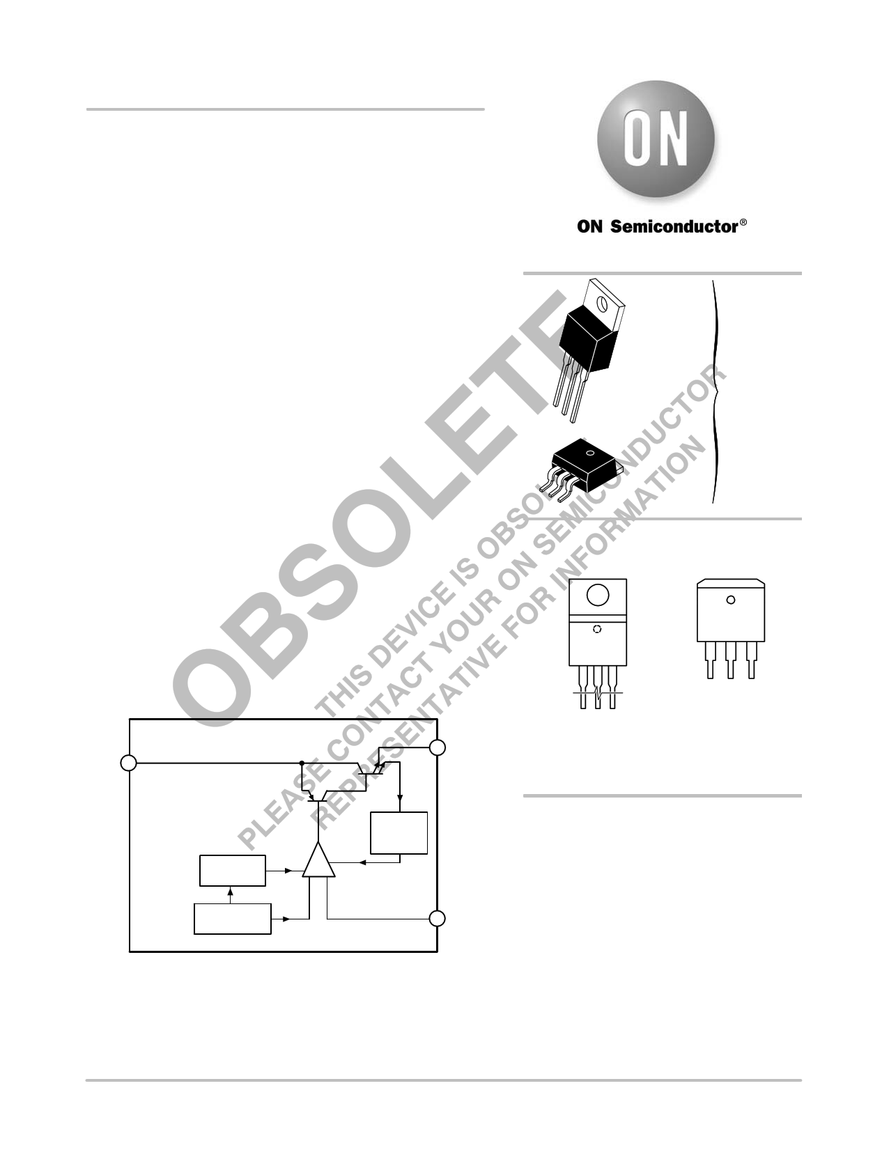
The regulator is available in TO−220−3 and surface mount
D2PAK−3 packages.
Features
• Output Current to 5.0 A
• Output Trimmed to ±1%
• Dropout Voltage 1.15 V @ 5.0 A
• Fast Transient Response
• Fault Protection Circuitry
− Thermal Shutdown
− Overcurrent Protection
− Safe Area Protection
VOUT
VIN
Thermal
Shutdown
Bandgap
Output
Current
Limit
− + Error
Amplifier
Adj
Figure 1. Block Diagram
http://onsemi.com
12 3
123
TO−220−3
T SUFFIX
CASE 221A
D2PAK−3
DP SUFFIX
CASE 418AB
Tab = VOUT
Pin 1. Adj
2. VOUT
3. VIN
MARKING DIAGRAMS
TO−220−3
D2PAK−3
CS5205A−1
AWLYWW
CS5205A−1
AWLYWW
1
1
A = Assembly Location
WL, L = Wafer Lot
YY, Y = Year
WW, W = Work Week
ORDERING INFORMATION
See detailed ordering and shipping information in the package
dimensions section on page 6 of this data sheet.
© Semiconductor Components Industries, LLC, 2006
September, 2006 − Rev. 7
1
Publication Order Number:
CS5205A−1/D
1 page 
CS5205A−1
VIN
C1
IN4002 (optional)
VIN VOUT
CS5205A−1
Adj
CAdj
VOUT
R1 C2
R2
Figure 8. Protection Diode Scheme for Adjustable
Output Regulator
Output Voltage Sensing
Since the CS5205A−1 is a three terminal regulator, it is not
possible to provide true remote load sensing. Load
regulation is limited by the resistance of the conductors
connecting the regulator to the load.
Best load regulation occurs when R1 is connected directly
to the output pin of the regulator as shown in Figure 9. If R1
is connected to the load, RC is multiplied by the divider ratio
and the effective resistance between the regulator and the
load becomes
ǒ ǓRC
R1 ) R2
R1
where RC = conductor parasitic resistance.
VIN VIN VOUT
Conductor Parasitic
RC Resistance
CS5205A−1
Adj
R1
RLOAD
R2
Figure 9. Grounding Scheme for Adjustable Output
Regulator to Minimize Parasitics
Calculating Power Dissipation and Heat Sink
Requirements
The CS5205A−1 linear regulator includes thermal shutdown
and safe operating area circuitry to protect the device. High
power regulators such as these usually operate at high junction
temperatures so it is important to calculate the power
dissipation and junction temperatures accurately to ensure that
an adequate heat sink is used.
The case is connected to VOUT on the CS5205A−1,
electrical isolation may be required for some applications.
Thermal compound should always be used with high current
regulators such as these.
The thermal characteristics of an IC depend on the
following four factors:
1. Maximum Ambient Temperature TA (°C)
2. Power dissipation PD (Watts)
3. Maximum junction temperature TJ (°C)
4. Thermal resistance junction to ambient RΘJA (°C/W)
These four are related by the equation
TJ + TA ) PD RQJA
(1)
The maximum ambient temperature and the power
dissipation are determined by the design while the
maximum junction temperature and the thermal resistance
depend on the manufacturer and the package type.
The maximum power dissipation for a regulator is:
PD(max) + {VIN(max) * VOUT(min)}IOUT(max) ) VIN(max)IQ
(2)
where:
VIN(max) is the maximum input voltage,
VOUT(min) is the minimum output voltage,
IOUT(max) is the maximum output current, for the application
IQ is the maximum quiescent current at IOUT(max).
A heat sink effectively increases the surface area of the
package to improve the flow of heat away from the IC and
into the surrounding air.
Each material in the heat flow path between the IC and the
outside environment has a thermal resistance. Like series
electrical resistances, these resistances are summed to
determine RΘJA, the total thermal resistance between the
junction and the surrounding air.
1. Thermal Resistance of the junction to case, RΘJC
(°C/W)
2. Thermal Resistance of the case to Heat Sink, RΘCS
(°C/W)
3. Thermal Resistance of the Heat Sink to the ambient
air, RΘSA (°C/W)
These are connected by the equation:
RQJA + RQJC ) RQCS ) RQSA
(3)
http://onsemi.com
5
5 Page | ||
| Páginas | Total 8 Páginas | |
| PDF Descargar | [ Datasheet CS5205A-1.PDF ] | |
Hoja de datos destacado
| Número de pieza | Descripción | Fabricantes |
| CS5205A-1 | 5A Adjustable Linear Regulator | Cherry Semiconductor Corporation |
| CS5205A-1 | 5.0A Adjustable Linear Regulator | ON Semiconductor |
| CS5205A-1GDP3 | 5A Adjustable Linear Regulator | Cherry Semiconductor Corporation |
| CS5205A-1GDPR3 | 5A Adjustable Linear Regulator | Cherry Semiconductor Corporation |
| Número de pieza | Descripción | Fabricantes |
| SLA6805M | High Voltage 3 phase Motor Driver IC. |
Sanken |
| SDC1742 | 12- and 14-Bit Hybrid Synchro / Resolver-to-Digital Converters. |
Analog Devices |
|
DataSheet.es es una pagina web que funciona como un repositorio de manuales o hoja de datos de muchos de los productos más populares, |
| DataSheet.es | 2020 | Privacy Policy | Contacto | Buscar |