|
|
|
PDF ASM1834 Data sheet ( Hoja de datos )
| Número de pieza | ASM1834 | |
| Descripción | Power Supply Supervisor | |
| Fabricantes | ON Semiconductor | |
| Logotipo | ||
Hay una vista previa y un enlace de descarga de ASM1834 (archivo pdf) en la parte inferior de esta página. Total 11 Páginas | ||
|
No Preview Available !
ASM1834, ASM1834A,
ASM1834D
Dual 5 V and 3.3 V mP
Power Supply Supervisor
with Manual Reset
Description
The ASM1834 supervisors simultaneously monitor both 3.3 V and
5 V power sources and generate reset signals when either supply is out
of tolerance. When an out−of−tolerance condition is detected, the
output−reset signal of the affected supply becomes active and resets
the system microprocessor/microcontroller. On power−up and after
the supply voltage returns to an in−tolerance condition, the reset signal
remains active for approximately 350 ms. This allows the power
supply and system microprocessor to stabilize.
Tolerance levels are independently selectable for both supplies.
Tolerance options are 5% and 10% for the 5 V supply and 10% and
20% for the 3.3 V supply.
The ASM1834 and ASM1834D have push−pull reset output stages.
The ASM1834A reset outputs are open drain devices that can both be
connected to either 5 V or 3.3 V supply. The ASM1834 and
ASM1834A have active LOW reset outputs. The ASM1834D has
active HIGH reset outputs.
All devices can generate reset signals through an internally
debounced pushbutton reset input that affects both reset outputs.
All devices operate over the extended industrial temperature range.
Devices are available in 8−pin DIP, surface mount 8−pin SO and 8−Pin
MicroSO packages. Die are also available.
http://onsemi.com
PDIP−8
NO SUFFIX
CASE 646AA
MICRO−8
U SUFFIX
CASE 846AA
SOIC−8
S SUFFIX
CASE 751BD
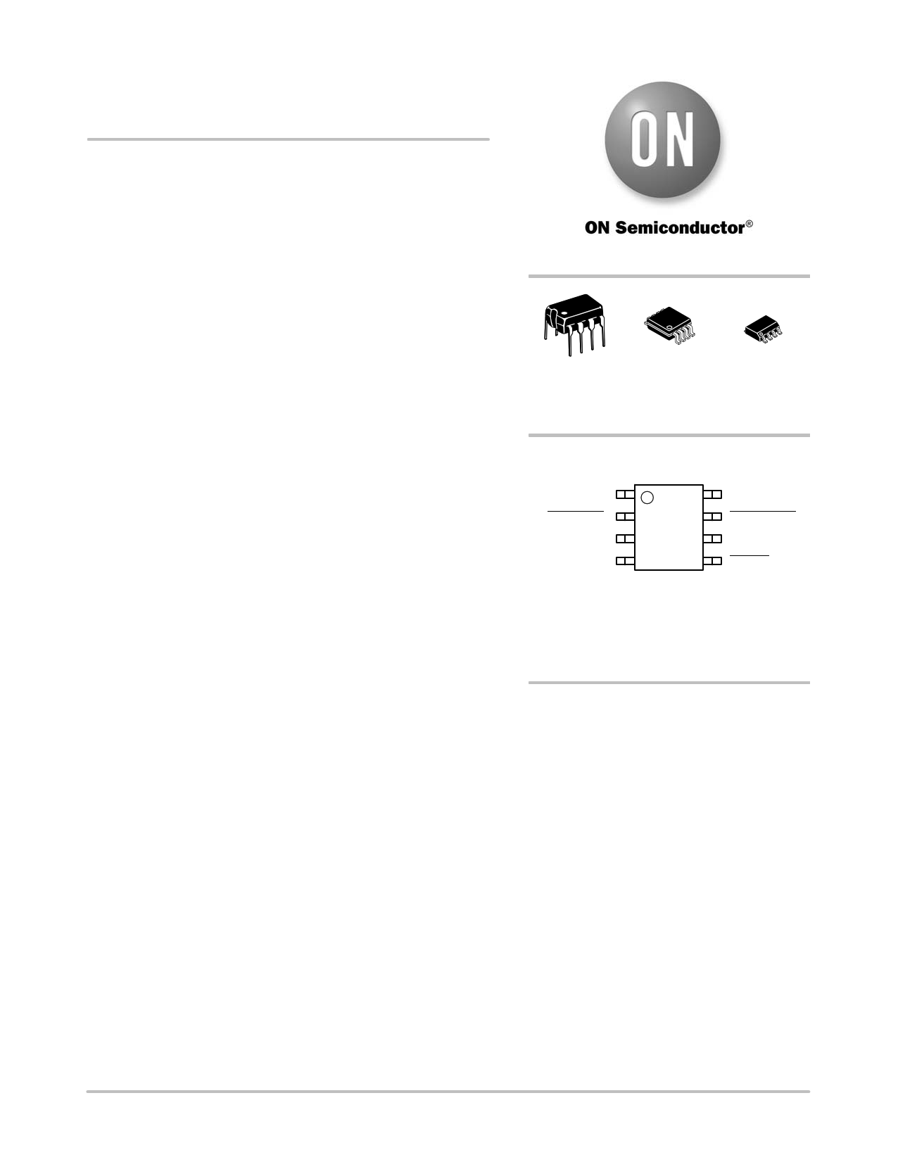
PIN CONFIGURATION
5VIN
5V RESET*
5V TOL
GND
1
ASM1834
ASM1834A
ASM1834D
(Top View)
3.3VIN
3.3V RESET*
3.3V TOL
PBRST
*AS1834D reset outputs are active HIGH
(5V RESET and 3.3V RESET) Outputs are
open−drain for AS1834A.
Features
• Monitors 5 V and 3.3 V Supplies Simultaneously
• 5 V and 3.3 V Power−on Reset
• 350 ms Reset Time
• Debounced Pushbutton Reset Input
• Push−pull CMOS Output
ASM1834, ASM1834D
Eliminates External Pull−up Resistors
Active LOW (ASM1834), HIGH (ASM1834D)
• Open Drain Output
ASM1834A
Active LOW
• Selectable 5 V and 3.3 V Trip Point Tolerance
• Internal Power Drawn from Highest Input Voltage,
5 V or 3.3 V
• Precision Temperature−compensated Voltage Reference
and Comparator
• Low Cost Surface Mount SO, Compact MicroSO and
DIP Packages
• Wide Operating Temperature: −40°C to +85°C
ORDERING INFORMATION
See detailed ordering and shipping information in the package
dimensions section on page 11 of this data sheet.
Applications
• Microprocessors
• PDAs, Hand−held PCs
• Embedded Controllers
• Telecommunication Systems
• Power Supplies
• Wireless / Cellular Systems
• Networking Hardware
© Semiconductor Components Industries, LLC, 2011
August, 2011 − Rev. 3
1
Publication Order Number:
ASM1834/D
1 page 
ASM1834, ASM1834A, ASM1834D
Detailed Description
Operation Power Monitor
The ASM1834 supervisors simultaneously detect
out−of−tolerance power supply conditions on both 3.3 V
and 5 V power supplies. If the voltages at 5VIN or 3.3VIN are
outside the tolerance band, the reset for the falling supply
voltage becomes active. When the monitored supply returns
to an intolerance state, the reset remains active for
approximately 350 ms before returning to the inactive state.
On power−up, the reset signals are kept active for
approximately 350 ms after the power supply voltages have
reached the selected tolerance. This allows the power supply
and microprocessor to stabilize before the reset is removed.
All supply current for the ASM1834 devices is drawn
from the input (5VIN or 3.3VIN) with the highest voltage
level. The outputs draw current from their input supplies
5VIN and 3.3VIN.
Figure 3. Timing Diagram: Power Up
(ASM1834D Only)
Figure 4. Timing Diagram: Power Down
(ASM1834D Only)
Reset Signal Polarity and Output Stage Structure
The ASM1834 and the ASM1834A supervisors have
active LOW reset signals. The ASM1834D reset outputs are
active HIGH.
The ASM1834 and the ASM1834D have CMOS
push−pull output stages. The ASM1834A has open drain
reset outputs.
Table 5.
Part #
ASM1834
ASM1834U
ASM1834S
ASM1834A
ASM1834AU
ASM1834AS
ASM1834D
ASM1834DU
ASM1834DS
RESET Polarity
LOW
LOW
LOW
LOW
LOW
LOW
HIGH
HIGH
HIGH
Output Stage Configuration
Push−Pull
Push−Pull
Push−Pull
Open Drain
Open Drain
Open Drain
Push−Pull
Push−Pull
Push−Pull
Manual Reset Operation
Push−button switch input, PBRST, allows the user to
override the internal trip point detection circuits and issue
reset signals. The pushbutton input is debounced and is
pulled HIGH through an internal 40 kW resistor.
When at least one of the reset outputs is not asserted, a
push button initiated reset signal can be issued by holding
PBRST LOW for at least 2 ms. When PBRST is held LOW,
both resets become active and remain active for
approximately 350 ms after PBRST returns HIGH. (See
Figures 5 and 6.)
http://onsemi.com
5
5 Page 
ASM1834, ASM1834A, ASM1834D
Table 7. ORDERING INFORMATION
Part Number
(Note 2)
Reset Polarity
Operating
Temperature Range
Output Stage
TIN − LEAD DEVICES
ASM1834
LOW
−40°C TO +85°C
Push−Pull
ASM1834U
LOW
−40°C TO +85°C
Push−Pull
ASM1834S
LOW
−40°C TO +85°C
Push−Pull
ASM1834A
LOW
−40°C TO +85°C
Open Drain
ASM1834AU
LOW
−40°C TO +85°C
Open Drain
ASM1834AS
LOW
−40°C TO +85°C
Open Drain
ASM1834D
HIGH
−40°C TO +85°C
Push−Pull
ASM1834DU
HIGH
−40°C TO +85°C
Push−Pull
ASM1834DS
HIGH
−40°C TO +85°C
Push−Pull
LEAD FREE DEVICES
ASM1834F
LOW
−40°C TO +85°C
Push−Pull
ASM1834UF
LOW
−40°C TO +85°C
Push−Pull
ASM1834SF
LOW
−40°C TO +85°C
Push−Pull
ASM1834AF
LOW
−40°C TO +85°C
Open Drain
ASM1834AUF
LOW
−40°C TO +85°C
Open Drain
ASM1834ASF
LOW
−40°C TO +85°C
Open Drain
ASM1834DF
HIGH
−40°C TO +85°C
Push−Pull
ASM1834DUF
HIGH
−40°C TO +85°C
Push−Pull
ASM1834DSF
HIGH
−40°C TO +85°C
Push−Pull
2. For parts to be packed in Tape and Reel, add “-T” at the end of the part number.
Package
8−DIP
MicroSO
8−SO
8−DIP
MicroSO
8−SO
8−DIP
MicroSO
8−SO
8−DIP
MicroSO
8−SO
8−DIP
MicroSO
8−SO
8−DIP
MicroSO
8−SO
Package Marking
ASM1834
ASM1834U
ASM1834S
ASM1834A
ASM1834AU
ASM1834AS
ASM1834D
ASM1834DU
ASM1834DS
ASM1834F
ASM1834UF
ASM1834SF
ASM1834AF
ASM1834AUF
ASM1834ASF
ASM1834DF
ASM1834DUF
ASM1834DSF
ON Semiconductor and
are registered trademarks of Semiconductor Components Industries, LLC (SCILLC). SCILLC reserves the right to make changes without further notice
to any products herein. SCILLC makes no warranty, representation or guarantee regarding the suitability of its products for any particular purpose, nor does SCILLC assume any liability
arising out of the application or use of any product or circuit, and specifically disclaims any and all liability, including without limitation special, consequential or incidental damages.
“Typical” parameters which may be provided in SCILLC data sheets and/or specifications can and do vary in different applications and actual performance may vary over time. All
operating parameters, including “Typicals” must be validated for each customer application by customer’s technical experts. SCILLC does not convey any license under its patent rights
nor the rights of others. SCILLC products are not designed, intended, or authorized for use as components in systems intended for surgical implant into the body, or other applications
intended to support or sustain life, or for any other application in which the failure of the SCILLC product could create a situation where personal injury or death may occur. Should
Buyer purchase or use SCILLC products for any such unintended or unauthorized application, Buyer shall indemnify and hold SCILLC and its officers, employees, subsidiaries, affiliates,
and distributors harmless against all claims, costs, damages, and expenses, and reasonable attorney fees arising out of, directly or indirectly, any claim of personal injury or death
associated with such unintended or unauthorized use, even if such claim alleges that SCILLC was negligent regarding the design or manufacture of the part. SCILLC is an Equal
Opportunity/Affirmative Action Employer. This literature is subject to all applicable copyright laws and is not for resale in any manner.
PUBLICATION ORDERING INFORMATION
LITERATURE FULFILLMENT:
Literature Distribution Center for ON Semiconductor
P.O. Box 5163, Denver, Colorado 80217 USA
Phone: 303−675−2175 or 800−344−3860 Toll Free USA/Canada
Fax: 303−675−2176 or 800−344−3867 Toll Free USA/Canada
Email: [email protected]
N. American Technical Support: 800−282−9855 Toll Free
USA/Canada
Europe, Middle East and Africa Technical Support:
Phone: 421 33 790 2910
Japan Customer Focus Center
Phone: 81−3−5773−3850
http://onsemi.com
11
ON Semiconductor Website: www.onsemi.com
Order Literature: http://www.onsemi.com/orderlit
For additional information, please contact your local
Sales Representative
ASM1834/D
11 Page | ||
| Páginas | Total 11 Páginas | |
| PDF Descargar | [ Datasheet ASM1834.PDF ] | |
Hoja de datos destacado
| Número de pieza | Descripción | Fabricantes |
| ASM1832 | 3.3V UP Power Supply Monitor and Reset Circuit | Alliance Semiconductor |
| ASM1832 | Power Supply Monitor and Reset Circuit | ON Semiconductor |
| ASM1834 | Dual 5V and 3.3V uP Power Supply Supervisor | Alliance Semiconductor |
| ASM1834 | Power Supply Supervisor | ON Semiconductor |
| Número de pieza | Descripción | Fabricantes |
| SLA6805M | High Voltage 3 phase Motor Driver IC. |
Sanken |
| SDC1742 | 12- and 14-Bit Hybrid Synchro / Resolver-to-Digital Converters. |
Analog Devices |
|
DataSheet.es es una pagina web que funciona como un repositorio de manuales o hoja de datos de muchos de los productos más populares, |
| DataSheet.es | 2020 | Privacy Policy | Contacto | Buscar |