|
|
|
PDF NCP6336 Data sheet ( Hoja de datos )
| Número de pieza | NCP6336 | |
| Descripción | Configurable 5.0A Step Down Converter | |
| Fabricantes | ON Semiconductor | |
| Logotipo | ||
Hay una vista previa y un enlace de descarga de NCP6336 (archivo pdf) en la parte inferior de esta página. Total 30 Páginas | ||
|
No Preview Available !
NCP6336
Product Preview
Configurable 5.0 A Step
Down Converter - Transient
Load Helper
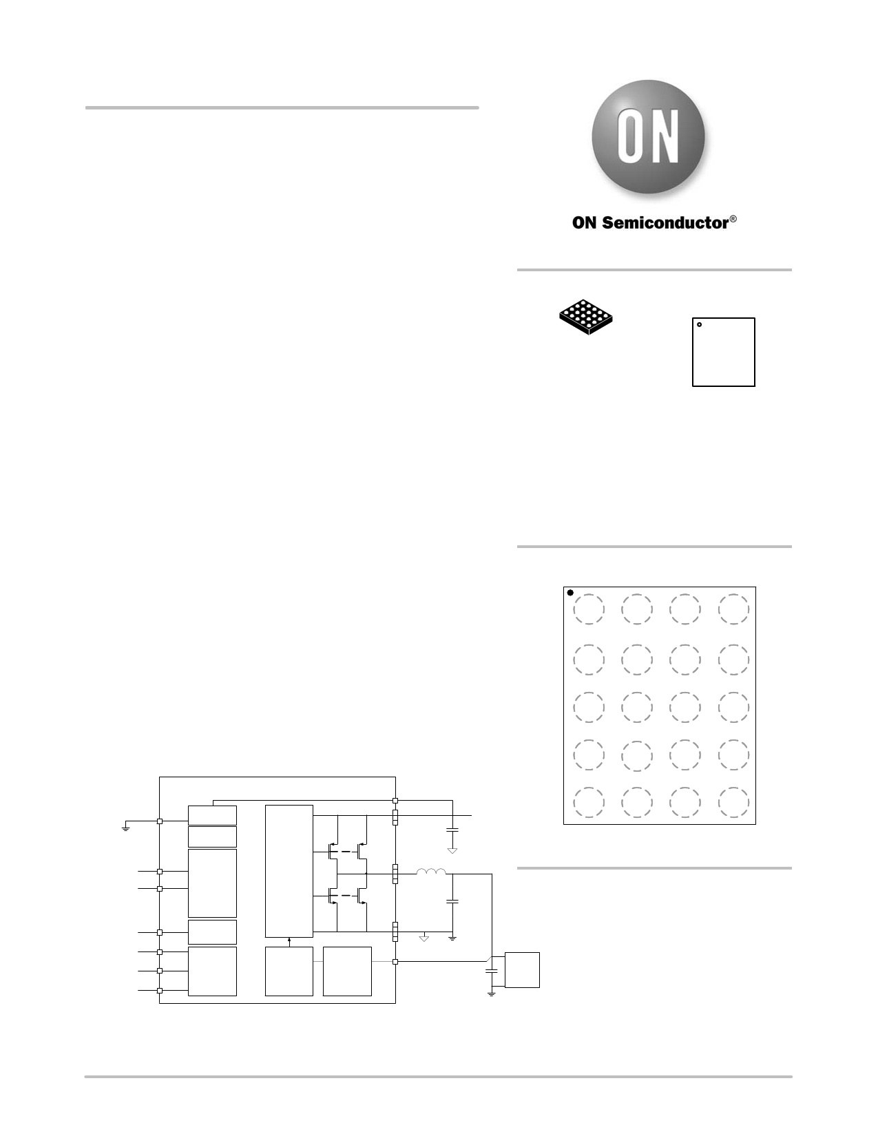
The NCP6336 is a synchronous buck converter optimized to supply
the different sub systems of portable applications powered by one cell
Li−Ion or three cell Alkaline/NiCd/NiMH batteries. The device is able
to deliver up to 5.0 A, with programmable output voltage from 0.6 V
to 1.5 V. It can share the same output rail with another DC−to−DC
converter and works as a transient load helper. Operation at a 3 MHz
switching frequency allows the use of small components.
Synchronous rectification and automatic PWM/PFM transitions
improve overall solution efficiency. The NCP6336 is in a space
saving, low profile 2.0 x 1.6 mm CSP−20 package.
Features
• Input Voltage Range from 2.3 V to 5.5 V: Battery and 5 V Rail
Powered Applications
• Programmable Output Voltage: 0.6 V to 1.5 V in 10 mV Steps
• 3 MHz Switching Frequency with On Chip Oscillator
• Uses 330 nH Inductor and 47 mF Capacitors for Optimized Footprint
and Solution Thickness
• PFM/PWM Operation for Optimum Increased Efficiency
• Low 35 mA Quiescent Current
• I2C Control Interface with Interrupt and Dynamic Voltage Scaling
Support
• Enable Pins, Power Good / Fail Signaling
• Thermal Protections and Temperature Management
• Transient Load Helper: Share the Same Rail with Another Rail
• Small 2.0 x 1.6 mm / 0.4 mm Pitch CSP Package
• These are Pb−Free Devices
http://onsemi.com
MARKING
DIAGRAM
WLCSP20
CASE 568AG
6336x
AWLYWW
G
x = P: Prototype
= blank: Production
A = Assembly Location
WL = Wafer Lot
Y = Year
WW = Work Week
G = Pb−Free Package
Pb−Free indicator, G or microdot (G), may or may
not be present
1
A VSEL
PIN OUT
23
EN SCL
4
FB
B SDA
PGND
INTB*
PGND
PG*
AGND
C PGND
PGND
PGND
PGND
Typical Applications
• Smartphones
• Tablets
D AVIN
PVIN
SW
SW
AGND B4
NCP6336
Core
Thermal
Protection
D1 AVIN
D2 PVIN
E1
E2
4.7 uF
Supply Input
E PVIN
PVIN
SW
(Top View)
*Optional
SW
Enable Control EN
Input
Voltage VSEL
Selection
A2
A1
Operating
Mode
Control
Power Fail
PGND
PG
B3
Interrupt
PGND
INTB
B2
SDA
Processor @IC
Control Interface SCL
B1
A3
Output
Monitoring
I@C
DCDC
5.0 A
DCDC
3 MHz
Controller
Sense
D3
D4
SW
E3
E4
330 nH
47 uF
C1
C2
PGND
C3
C4
A4 FB
ORDERING INFORMATION
See detailed ordering and shipping information on page 29 of
this data sheet.
Processor
Core
Figure 1. Typical Application Circuit
This document contains information on a product under development. ON Semiconductor
reserves the right to change or discontinue this product without notice.
© Semiconductor Components Industries, LLC, 2014
April, 2014 − Rev. P2
1
Publication Order Number:
NCP6336/D
1 page 
NCP6336
ELECTRICAL CHARACTERISTICS (Notes 10 and 11)
Min and Max Limits apply for TA = −40°C to +85°C, AVIN = PVIN = 3.6 V and default configuration, unless otherwise specified.
Typical values are referenced to TA = +25°C, AVIN = PVIN = 3.6 V and default configuration, unless otherwise specified.
Symbol
Parameter
Conditions
Min Typ Max
Unit
SUPPLY CURRENT: PINS AVIN – PVINx
IQ PWM
Operating quiescent current PWM DCDC active in Forced PWM
no load
− 15 25 mA
IQ PFM
Operating quiescent current PFM
DCDC active in Auto mode
no load − minimal switching
− 35 70 mA
ISLEEP
Product sleep mode current
IOFF Product in off mode
DC to DC CONVERTER
EN high, DCDC off or
EN low and (VSEL high or
Sleep_Mode high)
VIN = 2.5 V to 5.5 V
EN, VSEL and Sleep_Mode low
VIN = 2.5 V to 5.5 V
− 7 15 mA
− 0.8 5 mA
PVIN
IOUTMAX
Input Voltage Range
Maximum Output Current
Ipeak[1..0] = 00 (Note 12)
Ipeak[1..0] = 01 (Note 12)
2.3 − 5.5 V
3.5 − − A
4.0 − −
Ipeak[1..0] = 10 (Note 12)
4.5 − −
Ipeak[1..0] = 11 (Note 12)
5.0 − −
DVOUT
Output Voltage DC Error
FSW
RONHS
RONLS
IPK
Switching Frequency
P−Channel MOSFET On
Resistance
N−Channel MOSFET On
Resistance
Peak Inductor Current
Forced PWM mode, No load
Forced PWM mode, VIN range,
IOUT up to IOUTMAX (Note 12)
Auto mode, VIN range,
IOUT up to IOUTMAX (Note 12)
From PVIN to SW
VIN = 5.0 V
From SW to PGND
VIN = 5.0 V
Open loop – Ipeak[1..0] = 00 (Note 12)
Open loop – Ipeak[1..0] = 01 (Note 12)
−1
−1
−1
2.70
−
−
−
−
− 1%
−1
−2
3 3.30 MHz
23 40 mW
12 20 mW
5.2 −
5.8 −
A
Open loop – Ipeak[1..0] = 10 (Note 12) − 6.2 −
Open loop – Ipeak[1..0] = 11
6.1 6.8 7.8
DCLOAD
Load Regulation
IOUT from 0 A to IOUTMAX (Note 12)
Forced PWM mode
− −0.2 − %/A
DCLINE
Line Regulation
IOUT = 3 A
2.3 V ≤ VIN ≤ 5.5 V (Note 12)
Forced PWM mode
− 0 −%
ACLOAD
Transient Load Response
tr = ts = 100 ns
Load step 1.2 A (Note 12)
− ±40 − mV
D Maximum Duty Cycle
− 100 − %
tSTART
Turn on time
Time from EN transitions from Low to
High to 90% of Output Voltage
(DELAY[2..0] = 000b)
− 90 110 ms
RDISDCDC DCDC Active Output Discharge
VOUT = 1.15 V
−
25 35
W
9. Product parametric performance is indicated in the Electrical Characteristics for the listed test conditions, unless otherwise noted. Prod-
uct performance may not be indicated by the Electrical Characteristics if operated under different conditions.
10. Refer to the Application Information section of this data sheet for more details.
11. Devices that use non−standard supply voltages which do not conform to the intent I2C bus system levels must relate their input levels
to the VDD voltage to which the pull−up resistors RP are connected.
12. Guaranteed by design and characterized.
http://onsemi.com
5
5 Page 
NCP6336
TYPICAL OPERATING CHARACTERISTICS
AVIN = PVIN = 3.6 V, TJ = +25°C, DCDC = 1.15 V, Ipeak = 3.9 A (Unless otherwise noted). L = 0.33 mH PIFE25201B – COUT = 47 mF 0603,
CIN = 4.7 mF 0603
Figure 27. Transient Load 0.2 to 1.5 A
Transient Line 3.9 − 3.3 V Auto Mode
Figure 28. Transient Load 0.2 to 1.5 A
Transient Line 3.3 − 3.9 V Auto Mode
Figure 29. Transient Load 0.01 to 1.3 A Auto Mode
Figure 30. Transient Load 0.1 to 1.4 A Auto Mode
Figure 31. Transient Load 4 to 5.3 A Auto Mode
Figure 32. Transient Load 0 mA – 600 mA to
1.3 A − 1.9 A Auto Mode
http://onsemi.com
11
11 Page | ||
| Páginas | Total 30 Páginas | |
| PDF Descargar | [ Datasheet NCP6336.PDF ] | |
Hoja de datos destacado
| Número de pieza | Descripción | Fabricantes |
| NCP6332B | (NCP6332B/C) 1.2A Synchronous Buck Converter | ON Semiconductor |
| NCP6332C | (NCP6332B/C) 1.2A Synchronous Buck Converter | ON Semiconductor |
| NCP6334B | (NCP6334B/C) 2A Synchronous Buck Converter | ON Semiconductor |
| NCP6334C | (NCP6334B/C) 2A Synchronous Buck Converter | ON Semiconductor |
| Número de pieza | Descripción | Fabricantes |
| SLA6805M | High Voltage 3 phase Motor Driver IC. |
Sanken |
| SDC1742 | 12- and 14-Bit Hybrid Synchro / Resolver-to-Digital Converters. |
Analog Devices |
|
DataSheet.es es una pagina web que funciona como un repositorio de manuales o hoja de datos de muchos de los productos más populares, |
| DataSheet.es | 2020 | Privacy Policy | Contacto | Buscar |