|
|
|
PDF NYC222 Data sheet ( Hoja de datos )
| Número de pieza | NYC222 | |
| Descripción | Sensitive Gate Silicon Controlled Rectifiers | |
| Fabricantes | ON Semiconductor | |
| Logotipo | ||
Hay una vista previa y un enlace de descarga de NYC222 (archivo pdf) en la parte inferior de esta página. Total 5 Páginas | ||
|
No Preview Available !
NYC222, NYC226, NYC228
Sensitive Gate
Silicon Controlled Rectifiers
Reverse Blocking Thyristors
Designed and tested for repetitive peak operation required for CD
ignition, fuel ignitors, flash circuits, motor controls and low-power
switching applications.
Features
• Blocking Voltage to 600 V
• High Surge Current − 15 A
• Very Low Forward “On” Voltage at High Current
• Low-Cost Surface Mount SOT−223 Package
• These are Pb−Free Devices
MAXIMUM RATINGS (TJ = 25°C unless otherwise noted)
Rating
Symbol Value Unit
Peak Repetitive Off−State Voltage (Note 1)
(RGK = IK, TJ = *40 to +110°C, Sine Wave,
50 to 60 Hz, Gate Open)
NYC222
NYC226
NYC228
VDRM,
VRRM
50
400
600
V
On-State Current RMS
(180° Conduction Angles, TC = 80°C)
IT(RMS)
1.5
A
Average On−State Current,
(TC = 65°C, f = 60 Hz, Time = 1 sec)
IT(RMS)
2.0
A
Peak Non-repetitive Surge Current,
@TA = 25°C, (1/2 Cycle, Sine Wave, 60 Hz)
Circuit Fusing Considerations (t = 8.3 ms)
ITSM
I2t
15 A
0.9 A2s
Forward Peak Gate Power
(Pulse Width ≤ 1.0 msec, TA = 25°C)
PGM 0.5 W
Forward Average Gate Power
(t = 8.3 msec, TA = 25°C)
PG(AV)
0.1
W
Forward Peak Gate Current
(Pulse Width ≤ 1.0 ms, TA = 25°C)
IFGM 0.2 A
Reverse Peak Gate Voltage
(Pulse Width ≤ 1.0 ms, TA = 25°C)
Operating Junction Temperature Range
@ Rated VRRM and VDRM
VRGM
5.0
V
TJ −40 to +110 °C
Storage Temperature Range
Tstg −40 to +150 °C
Stresses exceeding those listed in the Maximum Ratings table may damage the
device. If any of these limits are exceeded, device functionality should not be
assumed, damage may occur and reliability may be affected.
1. VDRM and VRRM for all types can be applied on a continuous basis. Ratings
apply for zero or negative gate voltage; however, positive gate voltage shall
not be applied concurrent with negative potential on the anode. Blocking
voltages shall not be tested with a constant current source such that the
voltage ratings of the devices are exceeded.
© Semiconductor Components Industries, LLC, 2015
March, 2015 − Rev. 1
1
www.onsemi.com
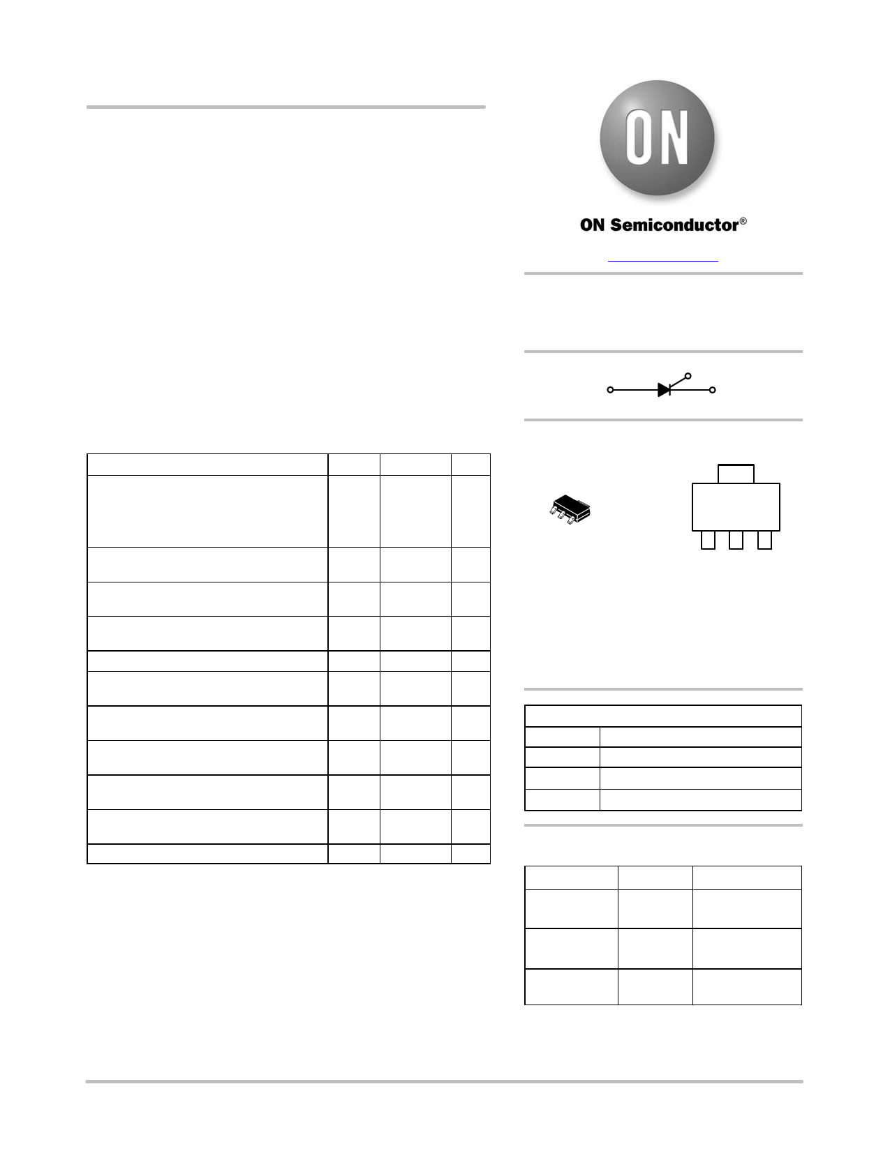
SCRs
1.5 AMPERES RMS
400 thru 600 VOLTS
G
AK
MARKING
DIAGRAM
SOT−223
CASE 318E
STYLE 11
1
AYW
22xSTG
G
A
Y
W
22xST
G
= Assembly Location
= Year
= Work Week
= Specific Device Code
x = 2, 6 or 8
= Pb−Free Package
(Note: Microdot may be in either location)
PIN ASSIGNMENT
1 K (Cathode)
2 A (Anode)
3 G (Gate)
4 A (Anode)
ORDERING INFORMATION
Device
NYC222STT1G
Package
SOT−223
(Pb−Free)
Shipping†
1000 /Tape & Reel
NYC226STT1G SOT−223 1000 /Tape & Reel
(Pb−Free)
NYC228STT1G SOT−223 1000 /Tape & Reel
(Pb−Free)
†For information on tape and reel specifications,
including part orientation and tape sizes, please
refer to our Tape and Reel Packaging Specification
Brochure, BRD8011/D.
Publication Order Number:
NYC222/D
1 page 
NYC222, NYC226, NYC228
PACKAGE DIMENSIONS
D
b1
4
HE
1 23
e1
e
0.08 (0003)
A1
E
b
A
SOT−223 (TO−261)
CASE 318E−04
ISSUE N
NOTES:
1. DIMENSIONING AND TOLERANCING PER ASME Y14.5M, 1994.
2. CONTROLLING DIMENSION: INCH.
MILLIMETERS
DIM MIN
NOM MAX
A 1.50
1.63
1.75
A1 0.02
0.06
0.10
b 0.60 0.75 0.89
b1 2.90
3.06
3.20
c 0.24 0.29 0.35
D 6.30
6.50
6.70
E 3.30
3.50
3.70
e 2.20 2.30 2.40
e1 0.85
0.94
1.05
L 0.20 −−− −−−
C
L1 1.50
1.75
2.00
q
H E 6.70
7.00
7.30
q 0°
− 10°
L L1
SOLDERING FOOTPRINT
3.8
0.15
MIN
0.060
0.001
0.024
0.115
0.009
0.249
0.130
0.087
0.033
0.008
0.060
0.264
0°
INCHES
NOM
0.064
0.002
0.030
0.121
0.012
0.256
0.138
0.091
0.037
−−−
0.069
0.276
−
MAX
0.068
0.004
0.035
0.126
0.014
0.263
0.145
0.094
0.041
−−−
0.078
0.287
10°
STYLE 11:
PIN 1. MT 1
2. MT 2
3. GATE
4. MT 2
2.0
0.079
2.3
0.091
2.3
0.091
6.3
0.248
2.0
0.079
1.5
0.059
ǒ ǓSCALE 6:1
mm
inches
ON Semiconductor and the are registered trademarks of Semiconductor Components Industries, LLC (SCILLC) or its subsidiaries in the United States and/or other countries.
SCILLC owns the rights to a number of patents, trademarks, copyrights, trade secrets, and other intellectual property. A listing of SCILLC’s product/patent coverage may be accessed
at www.onsemi.com/site/pdf/Patent−Marking.pdf. SCILLC reserves the right to make changes without further notice to any products herein. SCILLC makes no warranty, representation
or guarantee regarding the suitability of its products for any particular purpose, nor does SCILLC assume any liability arising out of the application or use of any product or circuit, and
specifically disclaims any and all liability, including without limitation special, consequential or incidental damages. “Typical” parameters which may be provided in SCILLC data sheets
and/or specifications can and do vary in different applications and actual performance may vary over time. All operating parameters, including “Typicals” must be validated for each
customer application by customer’s technical experts. SCILLC does not convey any license under its patent rights nor the rights of others. SCILLC products are not designed, intended,
or authorized for use as components in systems intended for surgical implant into the body, or other applications intended to support or sustain life, or for any other application in which
the failure of the SCILLC product could create a situation where personal injury or death may occur. Should Buyer purchase or use SCILLC products for any such unintended or
unauthorized application, Buyer shall indemnify and hold SCILLC and its officers, employees, subsidiaries, affiliates, and distributors harmless against all claims, costs, damages, and
expenses, and reasonable attorney fees arising out of, directly or indirectly, any claim of personal injury or death associated with such unintended or unauthorized use, even if such claim
alleges that SCILLC was negligent regarding the design or manufacture of the part. SCILLC is an Equal Opportunity/Affirmative Action Employer. This literature is subject to all applicable
copyright laws and is not for resale in any manner.
PUBLICATION ORDERING INFORMATION
LITERATURE FULFILLMENT:
Literature Distribution Center for ON Semiconductor
P.O. Box 5163, Denver, Colorado 80217 USA
Phone: 303−675−2175 or 800−344−3860 Toll Free USA/Canada
Fax: 303−675−2176 or 800−344−3867 Toll Free USA/Canada
Email: [email protected]
N. American Technical Support: 800−282−9855 Toll Free
USA/Canada
Europe, Middle East and Africa Technical Support:
Phone: 421 33 790 2910
Japan Customer Focus Center
Phone: 81−3−5817−1050
ON Semiconductor Website: www.onsemi.com
Order Literature: http://www.onsemi.com/orderlit
For additional information, please contact your local
Sales Representative
www.onsemi.com
5
NYC222/D
5 Page | ||
| Páginas | Total 5 Páginas | |
| PDF Descargar | [ Datasheet NYC222.PDF ] | |
Hoja de datos destacado
| Número de pieza | Descripción | Fabricantes |
| NYC222 | Sensitive Gate Silicon Controlled Rectifiers | ON Semiconductor |
| NYC226 | Sensitive Gate Silicon Controlled Rectifiers | ON Semiconductor |
| NYC228 | Sensitive Gate Silicon Controlled Rectifiers | ON Semiconductor |
| Número de pieza | Descripción | Fabricantes |
| SLA6805M | High Voltage 3 phase Motor Driver IC. |
Sanken |
| SDC1742 | 12- and 14-Bit Hybrid Synchro / Resolver-to-Digital Converters. |
Analog Devices |
|
DataSheet.es es una pagina web que funciona como un repositorio de manuales o hoja de datos de muchos de los productos más populares, |
| DataSheet.es | 2020 | Privacy Policy | Contacto | Buscar |