|
|
|
PDF NCP1249D Data sheet ( Hoja de datos )
| Número de pieza | NCP1249D | |
| Descripción | High-Voltage Current-Mode PWM Controller Featuring Peak Power Excursion and Self-Relaxing Off Mode | |
| Fabricantes | ON Semiconductor | |
| Logotipo | ||
Hay una vista previa y un enlace de descarga de NCP1249D (archivo pdf) en la parte inferior de esta página. Total 30 Páginas | ||
|
No Preview Available !
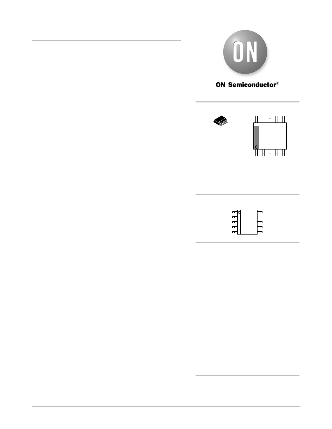
NCP1249C, NCP1249D
High-Voltage CurrentMode
PWM Controller Featuring
Peak Power Excursion and
Self-Relaxing Off Mode
The NCP1249 is a highly integrated high−voltage PWM controller
http://onsemi.com
capable of delivering a rugged and high performance offline power
supply with extremely low no−load consumption. With a supply range
MARKING DIAGRAM
up to 30 V, the controller hosts a jittered 65 kHz switching circuitry
operated in peak current mode control. When the power on the
secondary side starts to decrease, the controller automatically folds
back its switching frequency down to a minimum level of 26 kHz. As
the power further goes down, the part enters skip cycle while freezing
the peak current setpoint.
To help build rugged converters, the controller features several key
9
1
SOIC−9 NB
D SUFFIX
CASE 751BP
9
NCP1249x65
ALYW
G
1
protective features: a internal brown−out, a non−dissipative Over
Power Protection for a constant maximum output current regardless of
the input voltage and two latched over voltage protection inputs −
either through a dedicated pin or via the VCC input.
The controller architecture is arranged to authorize a transient peak
power excursion when the peak current hits the limit. At this point, the
XXXXX = Specific Device Code
A = Assembly Location
L = Wafer Lot
Y = Year
W = Work Week
G = Pb−Free Package
switching frequency is increased from 65 kHz to 130 kHz until the
PIN CONNECTIONS
peak requirement disappears. The timer duration is then modulated as
the converter crosses a peak power excursion mode (long) or
undergoes a short circuit (short).
Features
• High−Voltage Current Source for Lossless Start−up Sequence
X2
FB/REM
OPP/Latch
Timer
1
(Top View)
HV
VCC
DRV
GND
• Automatic and Lossless X2 Capacitors Discharge Function
• 65 kHz Fixed−Frequency Current−Mode Control Operation with
130 kHz Excursion
• Internal and Adjustable Over Power Protection (OPP)
• Up to 30 V VCC Maximum Rating
Circuit
• Internal Brown−Out Protection Circuit
• +300 mA/ −500 mA Source/Sink Drive Capability
• Extremely Low No−Load Standby Power via
• Frequency Foldback Down to 26 kHz and Skip−Cycle
Controlled Self−Relaxing Off Mode
in Light Load Conditions
• Adjustable Ramp Compensation
• Option for Auto−Recovery or Latched Short−Circuit
Protection
• Internally Fixed 4 ms Soft−Start
• Internal Thermal Shutdown with Hysteresis
• Adjustable Timer-Based Auto−Recovery
• These are Pb−Free Devices
Overload/Short−Circuit Protection
• 100% to 25% Timer Reduction from Overload to
Short−Circuit Fault
• Frequency Jittering in Normal and Frequency Foldback
Modes
Typical Applications
• Converters Requiring Peak−power Capability such as
Printers Power Supplies, ac−dc Adapters for Game
Stations
• Latched OVP Input for Improved Robustness and
Latched OVP on VCC
ORDERING INFORMATION
See detailed ordering and shipping information on page 2 of
this data sheet.
© Semiconductor Components Industries, LLC, 2013
September, 2013 − Rev. 0
1
Publication Order Number:
NCP1249C/D
1 page 
NCP1249C, NCP1249D
Table 4. ELECTRICAL CHARACTERISTICS (For typical values TJ = 25°C, for min/max values TJ = −40°C to +125°C,
Max TJ = 150°C, VCC = 12 V unless otherwise noted)
Symbol
Rating
Pin Min Typ Max
BROWN−OUT
V_BO_off
BO_Timer
Brown−Out turn−off threshold (VHV going down)
Timer duration for line cycle drop−out
10 84 93 102
10 40
− 100
X2 DISCHARGE CIRCUITRY
Vth_X2
Vth_X2_hyst
V_X2_clamp
X2_Timer
X2 timer disable switch threshold voltage
Hysteresis on the X2 pin
X2 input clamp voltage
X2 timer duration
1 1 1.5 2
1 − 100 −
1−4−
1 70 − 140
I_X2_leak
I_X2_dis
DRIVE OUTPUT
X2 input leakage current (V_X2 = 2.5 V)
Maximum discharge switch current (VCC = 10 V)
1 − − 0.3
10 6 10 13
Tr
Output voltage rise−time @ CL = 1 nF, 10−90% of output signal
7 − 40 80
Tf
Output voltage fall−time @ CL = 1 nF, 10−90% of output signal
7 − 30 70
ROH
Source resistance
7 − 13 −
ROL
Sink resistance
7−6−
Isource
Peak source current, VGS = 0 V (Note 2)
7 300
Isink
Peak sink current, VGS = 12 V (Note 2)
7 500
VDRV_low
DRV pin level at VCC close to VCC_OFF with a 33 kW resistor to GND
7
8
−
−
VDRV_high
DRV pin level at VCC= VOVP −0.2 V, DRV unloaded
7 10 12 14
CURRENT COMPARATOR
IIB
Vlimit
Vlimit
Input Bias Current @ 0.8 V input level on pin 3
Maximum internal current setpoint – TJ = 25°C – pin 4 grounded
Maximum internal current setpoint –
TJ from −40°C to 125°C – pin 4 grounded
3 0.02
3 0.744 0.8 0.856
3 0.72 0.8 0.88
Vfold_cs
Default internal voltage set point for
frequency foldback trip point ≈ 47% of Vlimit
3 475
Vfreeze_cs
TDEL
TLEB
TSS
IOPPo
IOOPv
Internal peak current setpoint freeze (≈31% of Vlimit)
Propagation delay from current detection to gate off−state
Leading Edge Blanking Duration
Internal soft−start duration activated upon startup, auto−recovery
Setpoint decrease for pin 5 biased to –250 mV – (Note 3)
Voltage setpoint for pin 5 biased to −250 mV – (Note 3)
TJ from −40°C to 125°C
3 250
3 100 150
3 300
−4
3 31.3
3 0.5 0.55 0.62
IOPPs
INTERNAL OSCILLATOR
Setpoint decrease for pin 4 grounded
30
fOSC_nom
Oscillation frequency, VFB < VFBtrans, pin 4 grounded
− 57 65 71
VFBtrans
Feedback voltage above which fsw increases
2 3.2
fOSC_max
Maximum oscillation frequency for VFB above VFBmax
− 115 130 140
VFBmax
Feedback voltage above which fsw is constant
2 3.8 4 4.2
Dmax
Maximum duty ratio
− 76 80 84
2. Guaranteed by design
3. See characterization table for linearity over negative bias voltage – we recommend keeping the level on pin 5 below −300 mV.
4. A 1 MW resistor is connected from pin 4 to the ground for the measurement.
Unit
V
ms
V
mV
V
ms
mA
mA
ns
ns
W
W
mA
mA
V
V
mA
V
V
mV
mV
ns
ns
ms
%
V
%
kHz
V
kHz
V
%
http://onsemi.com
5
5 Page 
NCP1249C, NCP1249D
TYPICAL CHARACTERISTICS
11.0 14.0
13.5
10.5
13.0
10.0
12.5
12.0
9.5
11.5
9.0
−40 −25 −10 5 20 35 50 65 80 95 110 125
TEMPERATURE (°C)
Figure 27. DRV Pin Level at VCC Close to
VCC_OFF, VDRV_low
0.85
11.0
−40 −25 −10 5 20 35 50 65 80 95 110 125
TEMPERATURE (°C)
Figure 28. DRV Pin Level at VCC Close to VOVP,
VDRV_high
500.0
0.83
490.0
0.81
480.0
0.79
470.0
0.77
460.0
0.75
−40 −25 −10 5 20 35 50 65 80 95 110 125
TEMPERATURE (°C)
Figure 29. Maximum Internal Current
Set−point, Vlimit
250.0
248.0
246.0
244.0
242.0
240.0
238.0
236.0
234.0
232.0
230.0
−40 −25 −10 5 20 35 50 65 80 95 110 125
TEMPERATURE (°C)
Figure 31. Internal Peak Current Set−point
Freeze, Vfreeze_CS
450.0
−40 −25 −10 5 20 35 50 65 80 95 110 125
TEMPERATURE (°C)
Figure 30. Default Internal Voltage Set Point
for Frequency Foldback, Vfold_CS
55
53
51
49
47
45
−40 −25 −10 5 20 35 50 65 80 95 110 125
TEMPERATURE (°C)
Figure 32. Propagation Delay from Current
Detection to Gate Off−state, TDEL
http://onsemi.com
11
11 Page | ||
| Páginas | Total 30 Páginas | |
| PDF Descargar | [ Datasheet NCP1249D.PDF ] | |
Hoja de datos destacado
| Número de pieza | Descripción | Fabricantes |
| NCP1249C | High-Voltage Current-Mode PWM Controller Featuring Peak Power Excursion and Self-Relaxing Off Mode | ON Semiconductor |
| NCP1249D | High-Voltage Current-Mode PWM Controller Featuring Peak Power Excursion and Self-Relaxing Off Mode | ON Semiconductor |
| Número de pieza | Descripción | Fabricantes |
| SLA6805M | High Voltage 3 phase Motor Driver IC. |
Sanken |
| SDC1742 | 12- and 14-Bit Hybrid Synchro / Resolver-to-Digital Converters. |
Analog Devices |
|
DataSheet.es es una pagina web que funciona como un repositorio de manuales o hoja de datos de muchos de los productos más populares, |
| DataSheet.es | 2020 | Privacy Policy | Contacto | Buscar |