|
|
PDF AP4203 Data sheet ( Hoja de datos )
| Número de pieza | AP4203 | |
| Descripción | 15ch 100mA LED Driver IC | |
| Fabricantes | AKM | |
| Logotipo |  |
|
Hay una vista previa y un enlace de descarga de AP4203 (archivo pdf) en la parte inferior de esta página. Total 28 Páginas | ||
|
No Preview Available !
[AP4203]
AP4203
15ch 100mA LED Driver IC
1. General Description
The AP4203 is a 15 channel LED Driver that supports 2 types of serial interfaces (SCI serial interface or serial
F/F cascade interface) to program LED lighting. The built-in 100mA drivable power MOSFET is used to shut
off the LED current, and LEDs are controlled by a PWM method in accordance with the LED gradation data
that is programmed into the device. Constant current output and Open drain output are selectable by DRSET
setting pin. To reduce wirings in the system, voltage on anode side of LEDs can be communized. A maximum
of 32 devices can be connected on a single BUS to a common master device; furthermore, each AP4203 retains
its own programmed commands allowing continuous autonomous lighting. The internal UVLO function
prevents the LEDs from incorrect operations when the supply voltage is 4V or less. An internal over current
protection function and a thermal protection function are also integrated.
2. Features
Power Supply Voltage 8.0V~24.0V
4.5V~5.5V (connect VIN pin and VDC1 pin)
Oprating Temperature 0 ~ 70C
Absolute Maximum Voltage 30V (VIN, LEDR4~8, LEDG4~8, LEDB4~8)
2 Types of Serial Interface for Setting Lighting Data
- 4-wire SCI interface (maximum communication clock: 5MHz)
- Serial-F/F cascade (maximum communication clock: 10MHz)
- Applicable to both 3.3V and 5.0V input signal (output is fixed to 5.0V)
LED Current maximum 100mA/ch
- Constant Current Output 50mA/ch
- Open Drain Output 100mA/ch
(Each channel current is less than the value when 15 channels are set simultaneously)
LED Gradation 8-bit PWM gradation method (256 gradation)
Built-in PWM Generator, Adjustable PWM Period
Simultaneous lighting-off function (SCI interface)
Protection Function
- Under voltage lock our (UVLO)
- Over current protection (timer latch recovery type)
- Thermal shutdown (automatic recovery)
Package 48-pin LQFP
Application A LED loading machine for the decoration
015008158-E-00
-1-
2015/09
1 page 
■ Function
No. Name
1 A3/CLRB
2 A4/ENB
3 CSB/LAT
4 SCK/CLK
5 TxD/SI
6 RxD/SO
7 DRSET
[AP4203]
Equivalent circuit
VDC1
VDC1
VDC1
VDC1
VDC1
VDC1
Explanation
IC address input pin 3 (built in 100kohm pull-up resistor).
Configure by connecting to GND or open.
CLRB input pin used for serial F/F.
Data clear pin used for shift register.
IC address input pin 4 (built in 100kohm pull-up resistor).
Configure by connecting to GND or open.
ENB input pin used for serial F/F.
Control the shift resister data which reflect to PWM data or
not.
Strobe signal input pin for SCI.
Respective orders are accepted when the CSB terminal goes
“L” level. The CSB terminal always needs to be “L” level
while commands are entered or data are transferred. If the CSB
pin goes “H” level when data are transferred, the commands
are disregarded.
LAT signal input pin used for serial F/F.
Input LAT signal for shift register.
Clock signal input for SCI.
Writing data is entered from the TxD pin at the SCK rising
edge, reading data is output to RxD pin at the SCK falling
edge. It is not always necessary to supply a clock signal to the
SCK pin.
CLK signal input pin used for serial F/F.
CLK signal for shift register.
Data signal input pin.
VDC1 To input commands, writing data.
SI input pin for serial F/F.
To input data signal of shift register.
Input to F/F which determine LEDB0 lighting data.
VDC1
Data signal output pin for SCI.
To output reading data.
Outputs Hi-Z except when data is output.
SO output pin for serial F/F.
To output data signal of shift register.
Output from F/F which determine LEDR8 lighting data.
VDC1
VDC1
Switching pin which can switch to driver output current source
or open drain (100kohm pull up)
Connect to GND or set to open.
If connect to GND, it can work as open drain mode.
015008158-E-00
-5-
2015/09
5 Page 
[AP4203]
■ SCI Interface (AC timing)
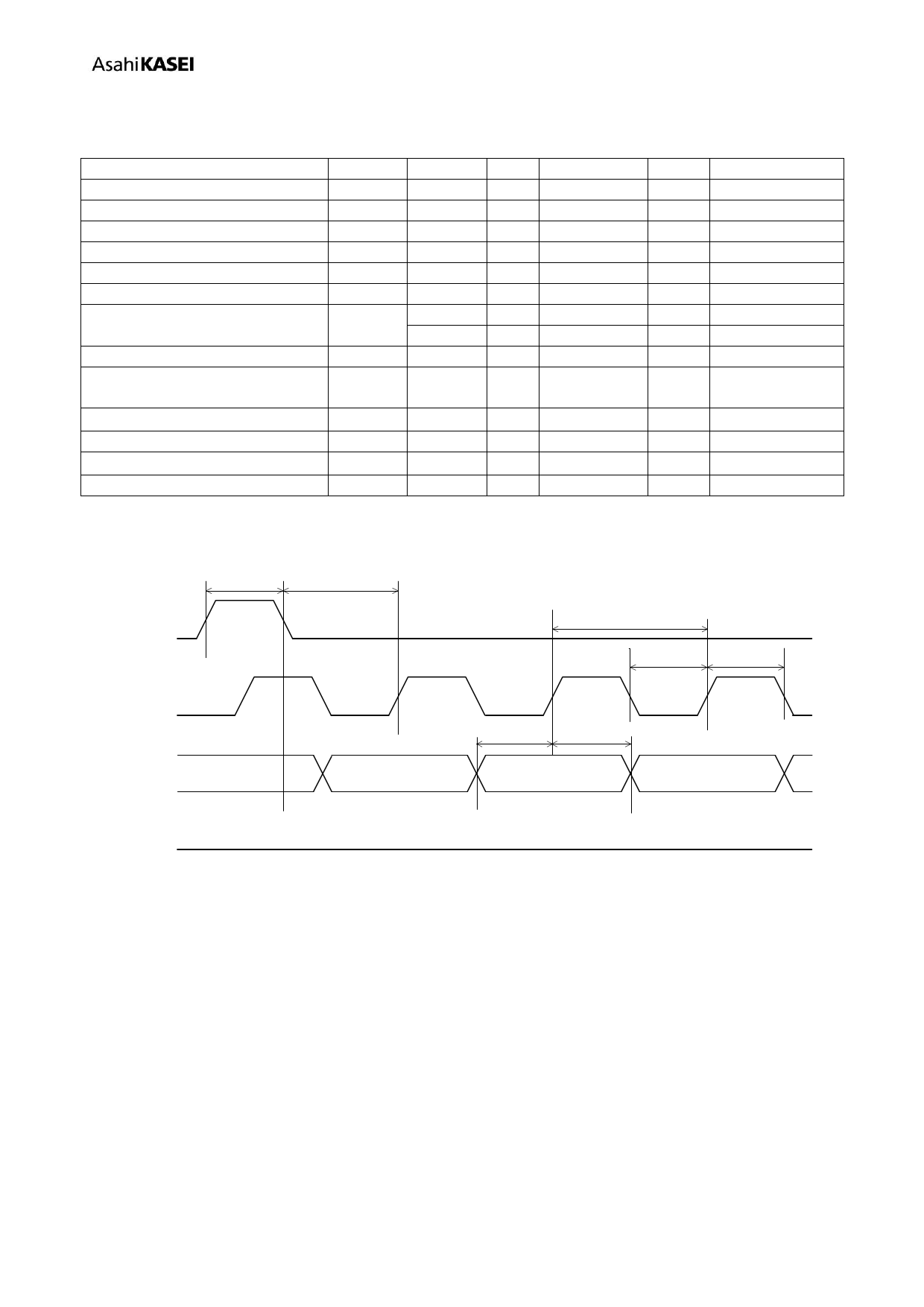
Table 1. SCI Timing
Parameter
Symbol min typ max Unit Condition
SCK Period
tSCKP 200 - - ns
SCK Pulse Width
tSCKW 60 - - ns
CSB Set-up Time
CSB Hold Time
tCSS 50 - - ns
tCSH 70 - - ns
Data Set-up Time
tDIS 50 - - ns
Data Hold Time
tDIH 70 - - ns
RxD pin Output Delay Time
tPD
--
--
80
50
ns CL=100pF
ns CL=20pF
CSB High-level Minimum Time
tCS
2-
-
μs
RxD pin High-impedance Output
Delay Time
tOZ
--
250
ns CL=100pF
SCK, CSB, TxD Raising Time
SCK, CSB, TxD Falling Time
tCSR
tCSF
- - tSCKW×15% ns tSCKW<4000ns
- - 600 ns tSCKW≥4000ns
- - tSCKW×15% ns tSCKW<4000ns
- - 600 ns tSCKW≥4000ns
CSB
SCK
TxD
RxD
tCS tCSS
tSCKP
tSCKW
tSCKW
tDIS tDIH
Hi-Z
Figure 2. SCI Interface Timing Chart 1
015008158-E-00
- 11 -
2015/09
11 Page | ||
| Páginas | Total 28 Páginas | |
| PDF Descargar | [ Datasheet AP4203.PDF ] | |
Hoja de datos destacado
| Número de pieza | Descripción | Fabricantes |
| AP4201 | 27ch 100mA LED Driver IC | AKM |
| AP4203 | 15ch 100mA LED Driver IC | AKM |
| Número de pieza | Descripción | Fabricantes |
| SLA6805M | High Voltage 3 phase Motor Driver IC. |
Sanken |
| SDC1742 | 12- and 14-Bit Hybrid Synchro / Resolver-to-Digital Converters. |
Analog Devices |
|
DataSheet.es es una pagina web que funciona como un repositorio de manuales o hoja de datos de muchos de los productos más populares, |
| DataSheet.es | 2020 | Privacy Policy | Contacto | Buscar |
