|
|
|
PDF SB3N551 Data sheet ( Hoja de datos )
| Número de pieza | SB3N551 | |
| Descripción | 3.3V / 5.0V Ultra-Low Skew 1:4 Clock Fanout Buffer | |
| Fabricantes | ON Semiconductor | |
| Logotipo | ||
Hay una vista previa y un enlace de descarga de SB3N551 (archivo pdf) en la parte inferior de esta página. Total 6 Páginas | ||
|
No Preview Available !
SB3N551
3.3 V / 5.0 V
Ultra-Low Skew
1:4 Clock Fanout Buffer
Description
The SB3N551 is a low skew 1−to−4 clock fanout buffer, designed
for clock distribution in mind. The SB3N551 specifically guarantees
low output−to−output skew. Optimal design, layout and processing
minimize skew within a device and from device to device.
The output enable (OE) pin three−states the outputs when low.
Features
• Input/Output Clock Frequency up to 160 MHz
• Low Skew Outputs (50 ps typical)
• RMS Phase Jitter (12 kHz – 20 MHz): 43 fs (Typical)
• Output goes to Three−State Mode via OE
• Operating Range: VDD = 3.0 V to 5.5 V
• Ideal for Networking Clocks
• Packaged in 8−pin SOIC
• Industrial Temperature Range
• These are Pb−Free Devices
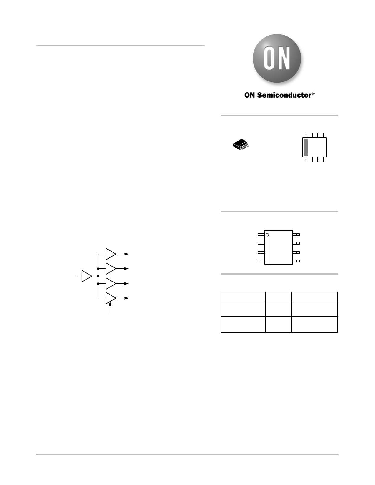
Q1
Q2
CLK
Q3
Q4
OE
Figure 1. Block Diagram
http://onsemi.com
8
1
SOIC−8
D SUFFIX
CASE 751
MARKING
DIAGRAMS*
8
3N551
ALYW
G
1
3N551 = Specific Device Code
A = Assembly Location
L = Wafer Lot
Y = Year
W = Work Week
G = Pb−Free Package
PIN CONNECTIONS
1
ICLK
2
Q1
3
Q2
4
Q3
8
OE
7
VDD
6
GND
5
Q4
ORDERING INFORMATION
Device
SB3N551DG
SB3N551DR2G
Package
Shipping†
SOIC−8
(Pb−Free)
98 Units/Rail
SOIC−8 2500/Tape & Reel
(Pb−Free)
†For information on tape and reel specifications,
including part orientation and tape sizes, please
refer to our Tape and Reel Packaging Specification
Brochure, BRD8011/D.
© Semiconductor Components Industries, LLC, 2015
January, 2015 − Rev. 0
1
Publication Order Number:
SB3N551/D
1 page 
SB3N551
Figure 2. Phase Noise Plot at 25 MHz at an Operating Voltage of 3.3 V, Room Temperature
The above plot captured using Agilent E5052A shows Additive Phase Noise of the SB3N551 device measured with an input
source generated by Agilent E8663B. The RMS phase jitter contributed by the device (integrated between 12 kHz to 20 MHz;
as shown in the shaded region of the plot) is 43 fs (RMS Jitter of the input source is 203.31 fs and Output (DUT+Source) is
247.06 fs).
Figure 3. Phase Noise Plot at 50 MHz at an Operating Voltage of 5 V, Room Temperature
The above plot captured using Agilent E5052A shows Additive Phase Noise of the SB3N551 device measured with an input
source generated by Agilent E8663B. The RMS phase jitter contributed by the device (integrated between 12 kHz to 20 MHz;
as shown in the shaded region of the plot) is 16 fs (RMS Jitter of the input source is 104.08 fs and Output (DUT + Source) is
119.77 fs).
http://onsemi.com
5
5 Page | ||
| Páginas | Total 6 Páginas | |
| PDF Descargar | [ Datasheet SB3N551.PDF ] | |
Hoja de datos destacado
| Número de pieza | Descripción | Fabricantes |
| SB3N551 | 3.3V / 5.0V Ultra-Low Skew 1:4 Clock Fanout Buffer | ON Semiconductor |
| Número de pieza | Descripción | Fabricantes |
| SLA6805M | High Voltage 3 phase Motor Driver IC. |
Sanken |
| SDC1742 | 12- and 14-Bit Hybrid Synchro / Resolver-to-Digital Converters. |
Analog Devices |
|
DataSheet.es es una pagina web que funciona como un repositorio de manuales o hoja de datos de muchos de los productos más populares, |
| DataSheet.es | 2020 | Privacy Policy | Contacto | Buscar |