|
|
PDF ICS854S058I Data sheet ( Hoja de datos )
| Número de pieza | ICS854S058I | |
| Descripción | 8:1 Differential-to-LVDS Clock Multiplexer | |
| Fabricantes | Integrated Device Technology | |
| Logotipo |  |
|
Hay una vista previa y un enlace de descarga de ICS854S058I (archivo pdf) en la parte inferior de esta página. Total 16 Páginas | ||
|
No Preview Available !
8:1 Differential-to-LVDS Clock Multiplexer
ICS854S058I
DATASHEET
General Description
The ICS854S058I is an 8:1 Differential-to-LVDS Clock Multiplexer
which can operate up to 2.5GHz. The ICS854S058I has 8
selectable differential clock inputs. The PCLK, nPCLK input pairs
can accept LVPECL, LVDS, SSTL or CML levels. The fully
differential architecture and low propagation delay make it ideal for
use in clock distribution circuits. The select pins have internal
pulldown resistors. The SEL2 pin is the most significant bit and the
binary number applied to the select pins will select the same
numbered data input (i.e., 000 selects PCLK0, nPCLK0).
Features
• High speed 8:1 differential multiplexer
• One differential LVDS output pair
• Eight selectable differential PCLK, nPCLK input pairs
• PCLKx, nPCLKx pairs can accept the following differential
input levels: LVPECL, LVDS, SSTL, CML
• Maximum output frequency: 2.5GHz
• Translates any single ended input signal to LVDS levels with
resistor bias on nPCLKx input
• Additive phase jitter, RMS: 0.065ps (typical)
• Part-to-part skew: 300ps (maximum)
• Propagation delay: 600ps (maximum)
• Supply voltage range: 3.135V to 3.465V
• -40°C to 85°C ambient operating temperature
• Available in lead-free (RoHS 6) packaging
Block Diagram
PCLK0 Pulldown
nPCLK0 Pullup/Pulldown
PCLK1 Pulldown
nPCLK1 Pullup/Pulldown
PCLK2 Pulldown
nPCLK2 Pullup/Pulldown
PCLK3 Pulldown
nPCLK3 Pullup/Pulldown
PCLK4 Pulldown
nPCLK4 Pullup/Pulldown
PCLK5 Pulldown
nPCLK5 Pullup/Pulldown
PCLK6 Pulldown
nPCLK6 Pullup/Pulldown
PCLK7 Pulldown
nPCLK7 Pullup/Pulldown
000
(default)
001
010
011
100
101
110
111
SEL2 Pulldown
SEL1 Pulldown
SEL0 Pulldown
Q
nQ
ICS854S058AGI REVISION A OCTOBER 29, 2012
Pin Assignment
PCLK0
nPCLK0
PCLK1
nPCLK1
VDD
SEL0
SEL1
SEL2
PCLK2
nPCLK2
PCLK3
nPCLK3
1
2
3
4
5
6
7
8
9
10
11
12
24 PCLK7
23 nPCLK7
22 PCLK6
21 nPCLK6
20 VDD
19 Q
18 nQ
17 GND
16 PCLK5
15 nPCLK5
14 PCLK4
13 nPCLK4
ICS854S058I
24-Lead TSSOP, 173-MIL
7.8mm x 4.4mm x 0.925mm package body
G Package
Top View
1 ©2012 Integrated Device Technology, Inc.
1 page 
ICS854S058I Datasheet
8:1, DIFFERENTIAL-TO-LVDS CLOCK MULTIPLEXER
Table 5. AC Characteristics, VDD = 3.3V ± 5%, TA = -40°C to 85°C
Symbol
Parameter
Test Conditions
fOUT
tPD
Output Frequency
Propagation Delay;
NOTE 1
tjit(Ø)
Buffer Additive Phase Jitter,
RMS; Refer to Additive Phase
Jitter Section
155.52MHz, Integration Range:
12kHz – 20MHz
tsk(pp)
Part-to-Part Skew;
NOTE 2, 3
tsk(i)
Input Skew
tR / tF
MUXISOLATION
Output Rise/Fall Time
MUX Isolation;
NOTE 4
20% to 80%
155.52MHz, VPP = 400mV
Minimum
300
75
Typical
0.065
85
Maximum
2.5
600
Units
GHz
ps
ps
300 ps
50 ps
250 ps
dB
NOTE: Electrical parameters are guaranteed over the specified ambient operating temperature range, which is established when the device
is mounted in a test socket with maintained transverse airflow greater than 500 lfpm. The device will meet specifications after thermal
equilibrium has been reached under these conditions.
All parameters measured 1.0GHz unless noted otherwise.
NOTE 1: Measured from the differential input crossing point to the differential output crossing point.
NOTE 2: Defined as skew between outputs on different devices operating at the same supply voltages and with equal load conditions. Using
the same type of inputs on each device, the outputs are measured at the differential cross points.
NOTE 3: This parameter is defined in accordance with JEDEC Standard 65.
NOTE 4: Q/nQ output measured differentially. See Parameter Measurement Information for MUX Isolation diagram.
ICS854S058AGI REVISION A OCTOBER 29, 2012
5
©2012 Integrated Device Technology, Inc.
5 Page 
ICS854S058I Datasheet
8:1, DIFFERENTIAL-TO-LVDS CLOCK MULTIPLEXER
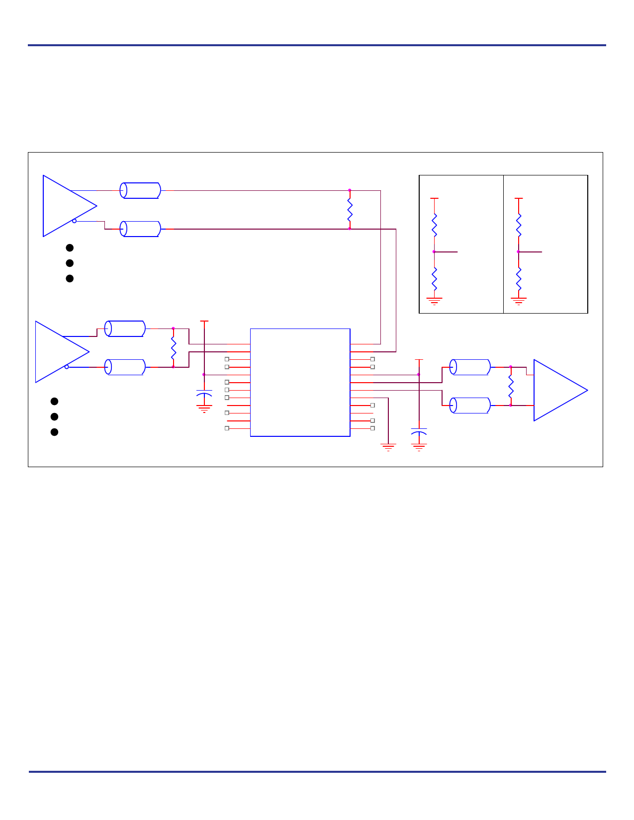
Schematic Example
An application schematic example of ICS854S058I is shown in
Figure 4. The inputs can accept various types of differential signals.
In this example, the inputs are driven by LVDS drivers. The
transmission lines are assumed to be 100 differential. The 100
matched loads termination should be located near the receivers. It is
recommended at least one decoupling capacitor per power pin. The
decoupling capacitor should be low ESR and located as close as
possible to the power pin.
Zo = 50
LVDS
Zo = 50
100 Ohm Differential
VDD=3.3V
100 Ohm Differential
Zo = 50
VDD
Zo = 50
R2
100
LVDS
C1
0.1u
U1
1
2 PCLK0
3 nPCLK0
4 PCLK1
5 nPCLK1
6 VDD
7 SEL0
8 SEL1
9 SEL2
10 PCLK2
11 nPCLK2
12 PCLK3
nPCLK3
ICS854S058
Figure 4. ICS854S058I Schematic Example
Logic Control Input Examples
Set Logic
Set Logic
R1 VDD Input to '1' VDD Input to '0'
100
RU1
1K
RU2
Not Install
To Logic
Input
pins
RD1
Not Install
To Logic
Input
pins
RD2
1K
PCLK7
nPCLK7
PCLK6
nPCLK6
VDD
Q
nQ
GND
PCLK5
nPCLK5
PCLK4
nPCLK4
24
23
22
21
20
19
18
17
16
15
14
13
VDD
Zo = 50
Zo = 50
R3
100
C2
0.1u
100 Ohm Differential
+
-
LVDS
ICS854S058AGI REVISION A OCTOBER 29, 2012
11
©2012 Integrated Device Technology, Inc.
11 Page | ||
| Páginas | Total 16 Páginas | |
| PDF Descargar | [ Datasheet ICS854S058I.PDF ] | |
Hoja de datos destacado
| Número de pieza | Descripción | Fabricantes |
| ICS854S058I | 8:1 Differential-to-LVDS Clock Multiplexer | Integrated Device Technology |
| Número de pieza | Descripción | Fabricantes |
| SLA6805M | High Voltage 3 phase Motor Driver IC. |
Sanken |
| SDC1742 | 12- and 14-Bit Hybrid Synchro / Resolver-to-Digital Converters. |
Analog Devices |
|
DataSheet.es es una pagina web que funciona como un repositorio de manuales o hoja de datos de muchos de los productos más populares, |
| DataSheet.es | 2020 | Privacy Policy | Contacto | Buscar |
