|
|
|
PDF GS1672 Data sheet ( Hoja de datos )
| Número de pieza | GS1672 | |
| Descripción | HD/SD-SDI Serializer | |
| Fabricantes | GENNUM | |
| Logotipo | ||
Hay una vista previa y un enlace de descarga de GS1672 (archivo pdf) en la parte inferior de esta página. Total 30 Páginas | ||
|
No Preview Available !
GS1672 HD/SD-SDI Serializer with Complete SMPTE Audio & Video Support
Key Features
• Operation at 1.485Gb/s, 1.485/1.001Gb/s and 270Mb/s
• Supports SMPTE 292, SMPTE 259M-C and DVB-ASI
• Integrated Cable Driver
• Integrated, low-noise VCO
• Integrated Narrow-Bandwidth PLL
• Integrated Audio Embedder for up to 8 channels of
48kHz audio
• Ancillary data insertion
• Parallel data bus selectable as either 20-bit or 10-bit
• SMPTE video processing including TRS calculation and
insertion, line number calculation and insertion, line
based CRC calculation and insertion, illegal code
re-mapping, SMPTE 352M payload identifier
generation and insertion
• GSPI host interface
• 1.2V digital core power supply, 1.2V and 3.3V analog
power supplies, and selectable 1.8V or 3.3V I/O power
supply
• -20ºC to +85ºC operating temperature range
• Low power operation (typically at 350mW, including
Cable Driver)
• Small 11mm x 11mm 100-ball BGA package
• Pb-free and RoHS compliant
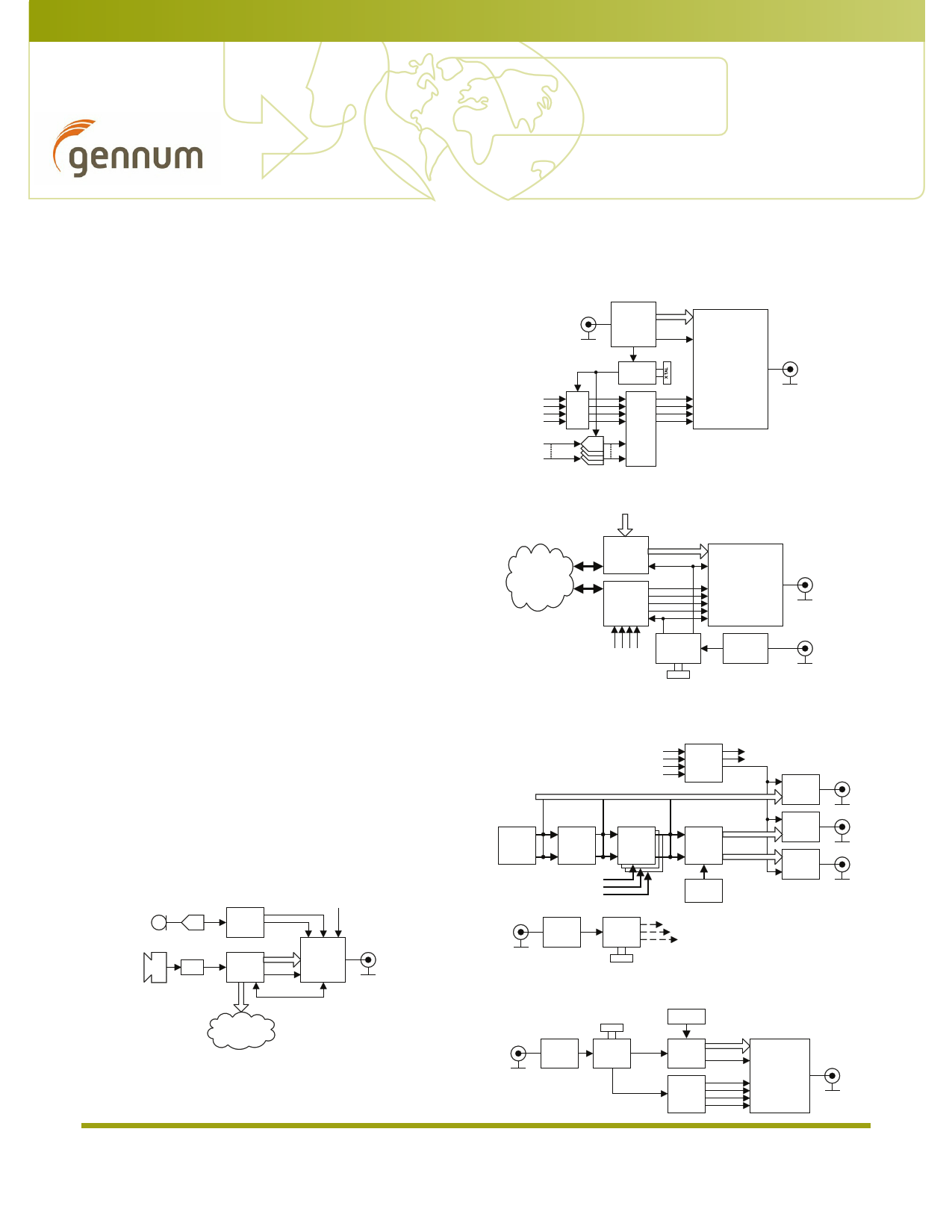
Applications
Application: 1080p 30 Camera/Camcorder
MIC
ADC
Audio
Processor
AUDIO 1/ 2
Audio Clocks
AES - IN
AUDIO 3/4
OPTICS
CCD
Video
Processor
20-bit
HV F/PCLK
GS1672
CTRL/TIME CODE
SD/HD-SDI
Storage :
Tape/Disc /Solid State
Application: Multi-format Audio Embedded Module
SD/HD-SDI
GS1670
HVF
10-bit
P CLK
Audio Clocks
GS4911
GS1672
SD/HD-SDI
AES
Audio
Inputs
Analog
Audio
Inputs
SRC
ADC
Switch
Logic
&
Buffers
AUDIO 1/ 2
AUDIO 3/ 4
AUDIO 5/ 6
AUDIO 7/ 8
Application: Multi-format Digital VTR/Video Server
V ideo Inputs
Storage :
Tape/HDD/Solid State
Video
Processor
Audio
Processor
20-bit
HV F/PCLK
A U D IO1/2
A U D IO3/4
A U D IO5/6
A U D IO7/8
Audio Clocks
GS1672
SD/HD-SDI
Audio Inputs
GS4911
X TAL
Sync
Seperator
Analog
Sync
Application: Multi-format Presentation Switcher
(Output Stage)
P rogram AE S In
P reset AE S In
V oice-Over
AE S from Input Dem ux
DVE
Mixers
KeyKK&eyeFeyriellr
Key/Fill
Inputs
Analog
Sync
Sync
Seperator
GS4911
X TAL
Audio
Mixer
P rogram AE S Out
P review AE S Out
I2C Audio + Clocks
10-bit + Clk
GS1672
SD/HD
Auxiliary
Logo
Inserter
20-bit + Clk
20-bit + Clk
GS1672
GS1672
SD/HD
Preview
SD/HD
Program
Image
Store
Clock &
Sync Distribution
Application: HD-SDI Test Signal Generator
Analog
Sync
Sync
Seperator
X TAL
GS4911
HV F/PCLK
Audio Clocks
Memory
Video
Signal
Generator
20-bit
HV F/PCLK
Audio
Generator
AES 1/2
AES 3/4
AES 5/6
AES 7/8
GS1672
HD-SDI
GS1672 HD/SD-SDI Serializer with Complete SMPTE
Audio & Video Support
Data Sheet
53623 - 6
July 2011
www.gennum.com
1 of 116
1 page 
4.7.15 Audio FIFO - HD.............................................................................................................. 51
4.7.16 Five-frame Sequence Detection - SD........................................................................ 52
4.7.17 Frame Sequence Detection - HD................................................................................ 55
4.7.18 ECC Error Detection and Correction ........................................................................ 56
4.7.19 Audio Control Packet Insertion - SD......................................................................... 56
4.7.20 Audio Control Packet Insertion - HD........................................................................ 57
4.7.21 Audio Data Packet Insertion........................................................................................ 58
4.7.22 Audio Interrupt Control ................................................................................................ 58
4.8 ANC Data Insertion ....................................................................................................................... 59
4.8.1 ANC Insertion Operating Modes .................................................................................. 60
4.8.2 HD ANC Insertion.............................................................................................................. 61
4.8.3 SD ANC Insertion............................................................................................................... 62
4.9 Additional Processing Functions .............................................................................................. 63
4.9.1 Video Format Detection .................................................................................................. 63
4.9.2 ANC Data Blanking ........................................................................................................... 65
4.9.3 ANC Data Checksum Calculation and Insertion..................................................... 66
4.9.4 TRS Generation and Insertion ....................................................................................... 66
4.9.5 HD Line Number Calculation and Insertion............................................................. 66
4.9.6 Illegal Code Re-Mapping................................................................................................. 66
4.9.7 SMPTE 352M Payload Identifier Packet Insertion.................................................. 67
4.9.8 Line Based CRC Generation and Insertion (HD)...................................................... 67
4.9.9 EDH Generation and Insertion...................................................................................... 67
4.9.10 HD HANC Space Considerations when Embedding Audio.............................. 68
4.9.11 Processing Feature Disable.......................................................................................... 69
4.10 352M Data Extraction ................................................................................................................ 69
4.11 Serial Clock PLL ........................................................................................................................... 71
4.11.1 PLL Bandwidth................................................................................................................. 71
4.11.2 Lock Detect........................................................................................................................ 72
4.12 Serial Digital Output .................................................................................................................. 72
4.12.1 Output Signal Interface Levels ................................................................................... 73
4.12.2 Overshoot/Undershoot ................................................................................................. 74
4.12.3 Slew Rate Selection......................................................................................................... 74
4.12.4 Serial Digital Output Mute ........................................................................................... 75
4.13 GSPI Host Interface ..................................................................................................................... 75
4.13.1 Command Word Description ...................................................................................... 76
4.13.2 Data Read or Write Access........................................................................................... 76
4.13.3 GSPI Timing....................................................................................................................... 77
4.14 Host Interface Register Maps .................................................................................................. 80
4.14.1 Video Core Registers...................................................................................................... 80
4.14.2 SD Audio Core.................................................................................................................. 90
4.14.3 HD Audio Core Registers............................................................................................ 101
4.15 JTAG ID Codeword ................................................................................................................... 109
4.16 JTAG Test Operation ................................................................................................................ 109
4.17 Device Power-Up ...................................................................................................................... 110
4.18 Device Reset ................................................................................................................................ 110
GS1672 HD/SD-SDI Serializer with Complete SMPTE
Audio & Video Support
Data Sheet
53623 - 6
July 2011
5 of 116
5 Page 
Table 1-1: Pin Descriptions (Continued)
Pin
Number
A4
A5, E1, G10,
K8
A6, B6
A7
A8
A9, D6, D7,
D8, F4
A10
B4
B5, C5, E2,
E5, E6, F5,
F6, G9
B7
Name
H/HSYNC
CORE_VDD
PLL_VDD
LF
VBG
RSV
A_VDD
PCLK
CORE_GND
VCO_VDD
Timing
Type
Description
Synch-
ronous
with
PCLK
Input
PARALLEL DATA TIMING.
Signal levels are LVCMOS / LVTTL compatible.
TIM_861 is LOW:
The H signal is used to indicate the portion of the video line
containing active video data, when DETECT_TRS is set LOW.
Active Line Blanking
The H signal should be LOW for the active portion of the video line.
The signal goes LOW at the first active pixel of the line, and then
goes HIGH after the last active pixel of the line.
The H signal should be set HIGH for the entire horizontal blanking
period, including both EAV and SAV TRS words, and LOW otherwise.
TRS Based Blanking (H_CONFIG = 1h)
The H signal should be set HIGH for the entire horizontal blanking
period as indicated by the H bit in the received TRS ID words, and
LOW otherwise.
TIM_861 = HIGH:
The HSYNC signal indicates horizontal timing. See Section 4.3.
When DETECT_TRS is HIGH, this pin is ignored at all times.
If DETECT_TRS is set HIGH and TIM_861 is set HIGH, the DETECT_TRS
feature will take priority.
Input Power Power supply connection for digital core logic. Connect to 1.2V DC
digital.
Input Power Power supply pin for PLL. Connect to 1.2V DC analog.
Analog
Output
Loop Filter component connection.
Output
Bandgap voltage filter connection.
− These pins are reserved and should be left unconnected.
Input Power VDD for sensitive analog circuitry. Connect to 3.3VDC analog.
Input
PARALLEL DATA BUS CLOCK.
Signal levels are LVCMOS / LVTTL compatible.
HD 20-bit mode
PCLK @ 74.25MHz
HD 10-bit mode
PCLK @ 148.5MHz
SD 20-bit mode
PCLK @ 13.5MHz
SD 10-bit mode
PCLK @ 27MHz
DVB-ASI mode
PCLK @ 27MHz
Input Power GND connection for digital logic. Connect to digital GND.
Input Power
Power pin for the VCO. Connect to a 1.2V±5% analog supply,
followed by a RC filter (see Typical Application Circuit on page 111).
A 105Ω 1% resistor must be used in the RC filter circuit. VCO_VDD is
nominally 0.7V.
GS1672 HD/SD-SDI Serializer with Complete SMPTE
Audio & Video Support
Data Sheet
53623 - 6
July 2011
11 of 116
11 Page | ||
| Páginas | Total 30 Páginas | |
| PDF Descargar | [ Datasheet GS1672.PDF ] | |
Hoja de datos destacado
| Número de pieza | Descripción | Fabricantes |
| GS1670 | HD/SD SDI Receiver Complete | Semtech |
| GS1670A | HD/SD SDI Receiver | Semtech |
| GS1671A | HD/SD SDI Receiver | Semtech |
| GS1672 | HD/SD-SDI Serializer | GENNUM |
| Número de pieza | Descripción | Fabricantes |
| SLA6805M | High Voltage 3 phase Motor Driver IC. |
Sanken |
| SDC1742 | 12- and 14-Bit Hybrid Synchro / Resolver-to-Digital Converters. |
Analog Devices |
|
DataSheet.es es una pagina web que funciona como un repositorio de manuales o hoja de datos de muchos de los productos más populares, |
| DataSheet.es | 2020 | Privacy Policy | Contacto | Buscar |