|
|
PDF F59D1G81A Data sheet ( Hoja de datos )
| Número de pieza | F59D1G81A | |
| Descripción | 1 Gbit (128M x 8/ 64M x 16) 1.8V NAND Flash Memory | |
| Fabricantes | Elite Semiconductor | |
| Logotipo | ||
Hay una vista previa y un enlace de descarga de F59D1G81A (archivo pdf) en la parte inferior de esta página. Total 30 Páginas | ||
|
No Preview Available !
ESMT
Flash
FEATURES
Voltage Supply: 1.8V (1.7 V ~ 1.95V)
Organization
x8:
- Memory Cell Array: (128M + 4M) x 8bit
- Data Register: (2K + 64) x 8bit
x16:
- Memory Cell Array: (64M + 2M) x 16bit
- Data Register: (1K + 32) x 16bit
Automatic Program and Erase
x8:
- Page Program: (2K + 64) Byte
- Block Erase: (128K + 4K) Byte
x16:
- Page Program: (1K + 32) Word
- Block Erase: (64K + 2K) Word
Page Read Operation
- Page Size: (2K + 64) Byte (x8)
Page Size: (1K + 32) Word (x16)
- Random Read: 25us (Max.)
- Serial Access: 45ns (Min.)
Memory Cell: 1bit/Memory Cell
Fast Write Cycle Time
- Program time: 250us (Typ.)
- Block Erase time: 2ms (Typ.)
Command/Address/Data Multiplexed I/O Port
F59D1G81A / F59D1G161A
1 Gbit (128M x 8/ 64M x 16)
1.8V NAND Flash Memory
Hardware Data Protection
- Program/Erase Lockout During Power Transitions
Reliable CMOS Floating Gate Technology
- ECC Requirement: x8 - 1bit/528Byte,
x16 - 1bit/264Word
- Endurance: 100K Program/Erase Cycles
- Data Retention: 10 Years
Command Register Operation
Automatic Page 0 Read at Power-Up Option
- Boot from NAND support
- Automatic Memory Download
NOP: 4 cycles
Cache Program Operation for High Performance Operation
Copy-Back Operation
EDO mode
OTP Operation
No Bad-Block-Erasing-Protect function (user should manage
bad blocks before erasing)
ORDERING INFORMATION
Product ID
x8:
F59D1G81A -45TG
F59D1G81A -45BG
x16:
F59D1G161A -45BG
Speed
45 ns
45 ns
45 ns
Package
48 pin TSOPI
63 ball BGA
63 ball BGA
Comments
Pb-free
Pb-free
Pb-free
Elite Semiconductor Memory Technology Inc.
Publication Date: May 2014
Revision: 1.5
1/43
1 page 
ESMT
F59D1G81A / F59D1G161A
Pin Description
Symbol
Pin Name
I/O0~I/O7 (x8)
I/O0~I/O15 (x16)
Data Inputs / Outputs
CLE
Command Latch
Enable
ALE Address Latch Enable
Functions
The I/O pins are used to input command, address and data, and to output data
during read operations. The I/O pins float to Hi-Z when the chip is deselected
or when the outputs are disabled.
The CLE input controls the activating path for commands sent to the command
register. When active high, commands are latched into the command register
through the I/O ports on the rising edge of the WE signal.
The ALE input controls the activating path for address to the internal address
registers. Addresses are latched on the rising edge of WE with ALE high.
CE Chip Enable
The CE input is the device selection control. When the device is in the Busy
state, CE high is ignored, and the device does not return to standby mode in
program or erase operation. Regarding CE control during read operation,
refer to ’Page read’ section of Device operation.
RE Read Enable
The RE input is the serial data-out control, and when active drives the data
onto the I/O bus. Data is valid tREA after the falling edge of RE which also
increments the internal column address counter by one.
WE Write Enable
The WE input controls writes to the I/O port. Commands, address and data
are latched on the rising edge of the WE pulse.
WP Write Protect
The WP pin provides inadvertent program/erase protection during power
transitions. The internal high voltage generator is reset when the WP pin is
active low.
R /B
VCC
VSS
NC
Ready / Busy Output
Power
Ground
No Connection
The R/ B output indicates the status of the device operation. When low, it
indicates that a program, erase or random read operation is in process and
returns to high state upon completion. It is an open drain output and does not
float to Hi-Z condition when the chip is deselected or when outputs are
disabled.
VCC is the power supply for device.
Lead is not internally connected.
Note: Connect all VCC and VSS pins of each device to common power supply outputs. Do not leave VCC or VSS disconnected.
Elite Semiconductor Memory Technology Inc.
Publication Date: May 2014
Revision: 1.5
5/43
5 Page 
ESMT
F59D1G81A / F59D1G161A
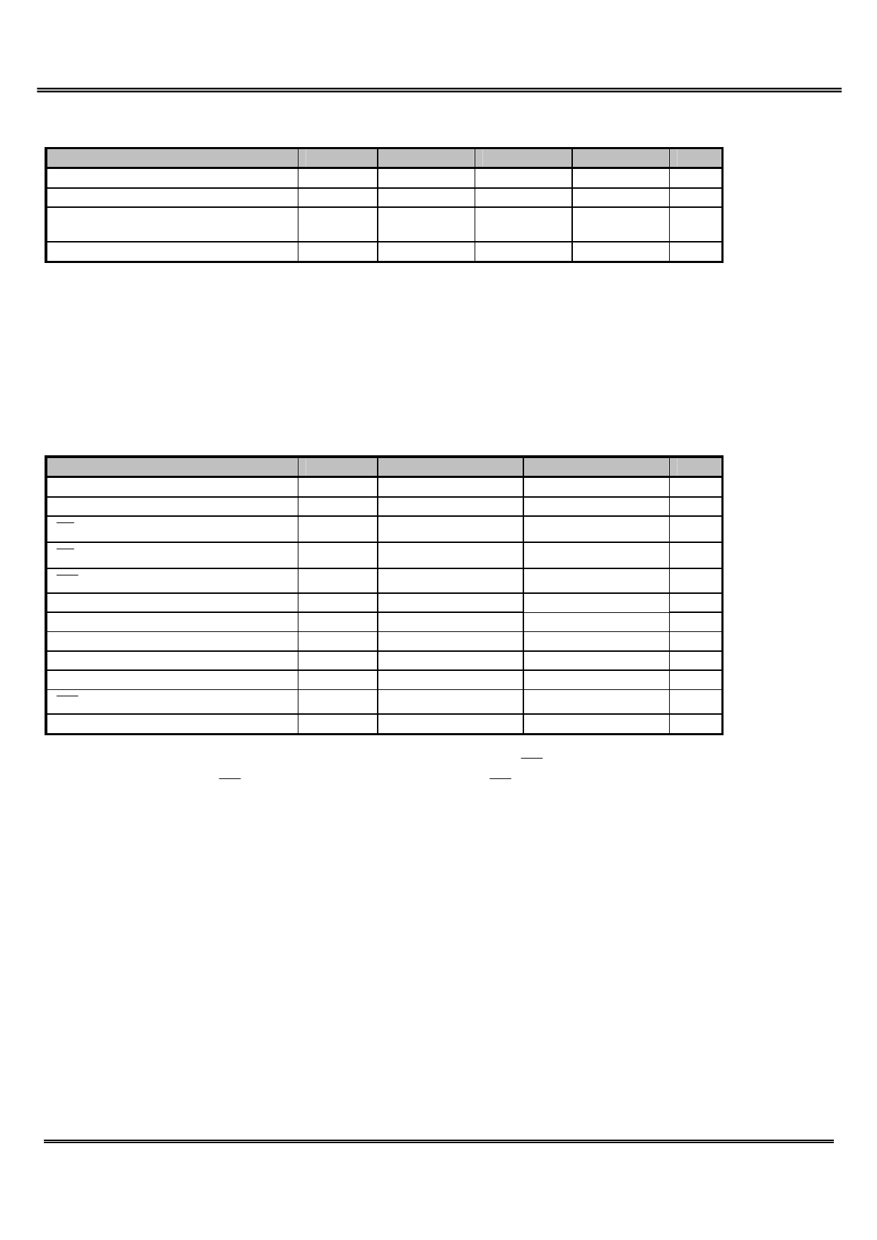
Program / Erase Characteristics
(TA=0 to 70℃, VCC=1.7V~1.95V)
Parameter
Symbol
Min.
Typ.
Max.
Unit
Program Time
Dummy Busy Time for Cache Program
Number of Partial Program Cycles in the
Same Page
tPROG
tCBSY
NOP
-
-
-
250 700 us
3 700 us
- 4 Cycle
Block Erase Time
tBERS
-
2 10 ms
Note:
1. Typical program time is defined as the time within which more than 50% of the whole pages are programmed at 1.8V VCC and 25℃
temperature.
2. tPROG is the average program time of all pages. Users should be noted that the program time variation from page to page is
possible.
3. tCBSY max. time depends on timing between internal program completion and data in.
AC Timing Characteristics for Command / Address / Data Input
Parameter
CLE Setup Time
CLE Hold Time
CE Setup Time
Symbol
tCLS(1)
tCLH
tCS(1)
Min.
25
10
35
Max.
-
-
-
Unit
ns
ns
ns
CE Hold Time
tCH 10
- ns
WE Pulse Width
ALE Setup Time
ALE Hold Time
Data Setup Time
Data Hold Time
Write Cycle Time
tWP
tALS(1)
tALH
tDS(1)
tDH
tWC
25
25
10
20
10
45
- ns
- ns
- ns
- ns
- ns
- ns
WE High Hold Time
ALE to Data Loading Time
tWH
tADL(2)
15
100
- ns
- ns
Note:
1. The transition of the corresponding control pins must occur only once while WE is held low.
2. tADL is the time from the WE rising edge of final address cycle to the WE rising edge of first data cycle.
Elite Semiconductor Memory Technology Inc.
Publication Date: May 2014
Revision: 1.5
11/43
11 Page | ||
| Páginas | Total 30 Páginas | |
| PDF Descargar | [ Datasheet F59D1G81A.PDF ] | |
Hoja de datos destacado
| Número de pieza | Descripción | Fabricantes |
| F59D1G81A | 1 Gbit (128M x 8/ 64M x 16) 1.8V NAND Flash Memory | Elite Semiconductor |
| Número de pieza | Descripción | Fabricantes |
| SLA6805M | High Voltage 3 phase Motor Driver IC. |
Sanken |
| SDC1742 | 12- and 14-Bit Hybrid Synchro / Resolver-to-Digital Converters. |
Analog Devices |
|
DataSheet.es es una pagina web que funciona como un repositorio de manuales o hoja de datos de muchos de los productos más populares, |
| DataSheet.es | 2020 | Privacy Policy | Contacto | Buscar |
