|
|
|
PDF SQ3426EV Data sheet ( Hoja de datos )
| Número de pieza | SQ3426EV | |
| Descripción | Automotive N-Channel MOSFET | |
| Fabricantes | Vishay | |
| Logotipo | ||
Hay una vista previa y un enlace de descarga de SQ3426EV (archivo pdf) en la parte inferior de esta página. Total 8 Páginas | ||
|
No Preview Available !
www.vishay.com
SQ3426EV
Vishay Siliconix
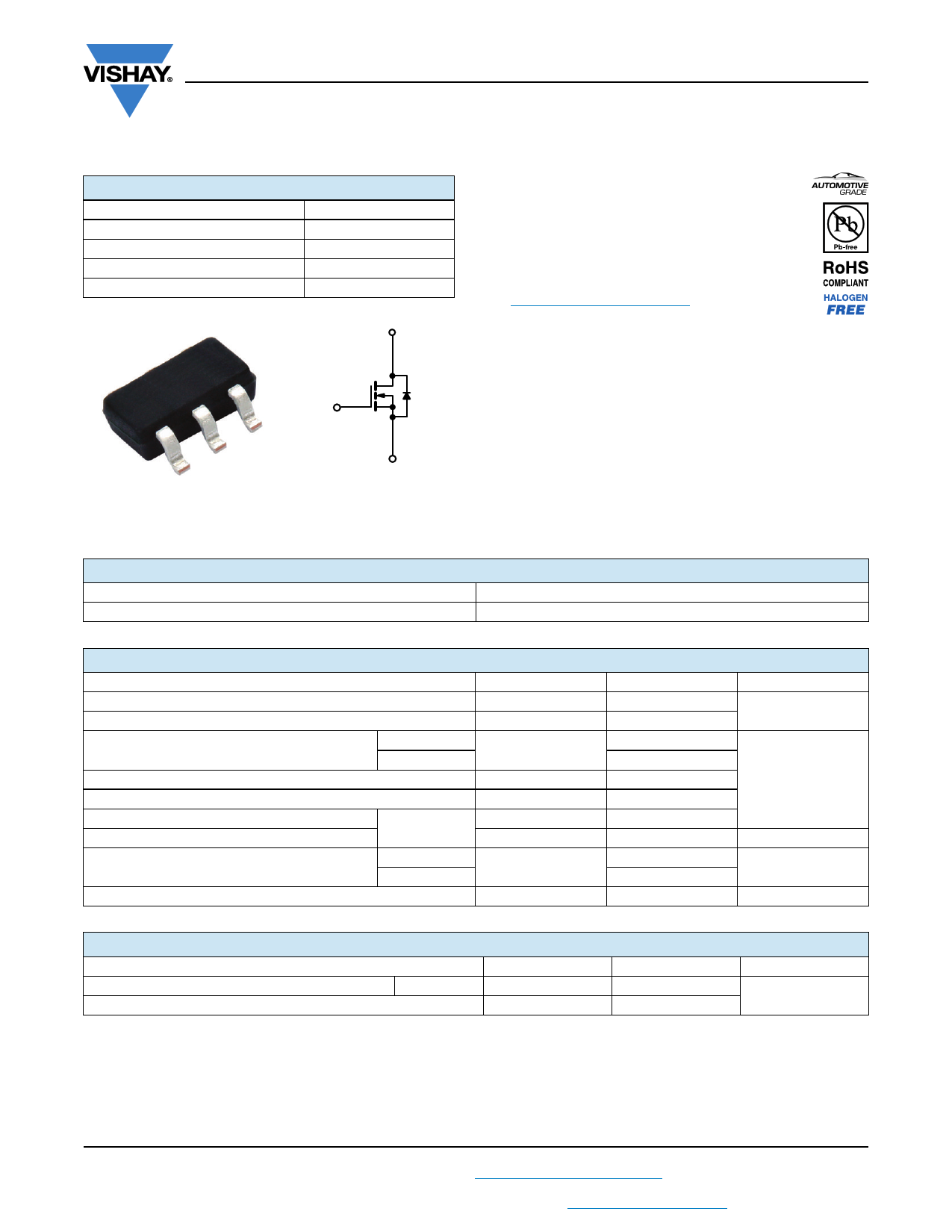
Automotive N-Channel 60 V (D-S) 175 °C MOSFET
PRODUCT SUMMARY
VDS (V)
RDS(on) (Ω) at VGS = 10 V
RDS(on) (Ω) at VGS = 4.5 V
ID (A)
Configuration
TSOP-6 Single
S
4
D
5
D
6
1
D
Top View
Marking Code: 8Q
2
D
3
G
60
0.042
0.063
7
Single
(1, 2, 5, 6) D
(3) G
(4) S
N-Channel MOSFET
FEATURES
• TrenchFET® power MOSFET
• AEC-Q101 qualified
• 100 % Rg and UIS tested
• Material categorization:
for definitions of compliance please see
www.vishay.com/doc?99912
ORDERING INFORMATION
Package
Lead (Pb)-free and Halogen-free
TSOP-6
SQ3426EV-T1-GE3
ABSOLUTE MAXIMUM RATINGS (TC = 25 °C, unless otherwise noted)
PARAMETER
SYMBOL
Drain-Source Voltage
Gate-Source Voltage
Continuous Drain Current
Continuous Source Current (Diode Conduction)
TC = 25 °C
TC = 125 °C
Pulsed Drain Current a
Single Pulse Avalanche Current
Single Pulse Avalanche Energy
L = 0.1 mH
Maximum Power Dissipation a
TC = 25 °C
TC = 125 °C
Operating Junction and Storage Temperature Range
VDS
VGS
ID
IS
IDM
IAS
EAS
PD
TJ, Tstg
LIMIT
60
± 20
7
4
6
29
10
5
5
1.6
- 55 to +175
THERMAL RESISTANCE RATINGS
PARAMETER
Junction-to-Ambient
Junction-to-Foot (Drain)
Notes
a. Pulse test; pulse width ≤ 300 μs, duty cycle ≤ 2 %.
b. When mounted on 1" square PCB (FR4 material).
PCB Mount b
SYMBOL
RthJA
RthJF
LIMIT
110
30
UNIT
V
A
mJ
W
°C
UNIT
°C/W
S15-2119-Rev. B, 07-Sep-15
1
Document Number: 65107
For technical questions, contact: [email protected]
THIS DOCUMENT IS SUBJECT TO CHANGE WITHOUT NOTICE. THE PRODUCTS DESCRIBED HEREIN AND THIS DOCUMENT
ARE SUBJECT TO SPECIFIC DISCLAIMERS, SET FORTH AT www.vishay.com/doc?91000
1 page 
www.vishay.com
THERMAL RATINGS (TA = 25 °C, unless otherwise noted)
SQ3426EV
Vishay Siliconix
1
Duty Cycle = 0.5
IDM Limited
10
Limited by RDS(on)*
100 μs
1 ms
1
10 ms
0.1
TC = 25 °C
Single Pulse
BVDSS Limited
100 ms
1 s,
10 s, DC
0.01
0.01
0.1
1
10 100
VDS - Drain-to-Source Voltage (V)
* VGS > minimum VGS at which RDS(on) is specified
Safe Operating Area
0.2
0.1
0.1
0.05
0.02
Single Pulse
0.01
10-4
10-3
Notes:
PDM
t1
t2
1. Duty Cycle, D =
t1
t2
2. Per Unit Base = RthJA = 110 °C/W
3. TJM - TA = PDMZthJA(t)
4. Surface Mounted
10-2
10-1
1
10
Square Wave Pulse Duration (s)
Normalized Thermal Transient Impedance, Junction-to-Ambient
100
1000
S15-2119-Rev. B, 07-Sep-15
5
Document Number: 65107
For technical questions, contact: [email protected]
THIS DOCUMENT IS SUBJECT TO CHANGE WITHOUT NOTICE. THE PRODUCTS DESCRIBED HEREIN AND THIS DOCUMENT
ARE SUBJECT TO SPECIFIC DISCLAIMERS, SET FORTH AT www.vishay.com/doc?91000
5 Page | ||
| Páginas | Total 8 Páginas | |
| PDF Descargar | [ Datasheet SQ3426EV.PDF ] | |
Hoja de datos destacado
| Número de pieza | Descripción | Fabricantes |
| SQ3426EEV | Automotive N-Channel MOSFET | Vishay |
| SQ3426EV | Automotive N-Channel MOSFET | Vishay |
| Número de pieza | Descripción | Fabricantes |
| SLA6805M | High Voltage 3 phase Motor Driver IC. |
Sanken |
| SDC1742 | 12- and 14-Bit Hybrid Synchro / Resolver-to-Digital Converters. |
Analog Devices |
|
DataSheet.es es una pagina web que funciona como un repositorio de manuales o hoja de datos de muchos de los productos más populares, |
| DataSheet.es | 2020 | Privacy Policy | Contacto | Buscar |