|
|
|
PDF LTC4308 Data sheet ( Hoja de datos )
| Número de pieza | LTC4308 | |
| Descripción | Level Shifting Hot Swappable 2-Wire Bus Buffer | |
| Fabricantes | Linear | |
| Logotipo | ||
Hay una vista previa y un enlace de descarga de LTC4308 (archivo pdf) en la parte inferior de esta página. Total 16 Páginas | ||
|
No Preview Available !
LTC4308
Low Voltage, Level Shifting
Hot Swappable 2-Wire Bus
Buffer with Stuck Bus Recovery
FEATURES
DESCRIPTION
n Optimized for Low Voltage Systems Down to 0.9V
n Bidirectional Buffer with Stuck Bus Recovery
n –200mV Offset In-Out/+300mV Offset Out-In
n 30ms Stuck Bus Timeout
n Compatible with Non-Compliant VOL I2C Devices
n Prevents SDA and SCL Corruption During Live
Board Insertion and Removal from Backplane
n ±6kV Human Body Model (HBM) ESD Protection
n Isolates Input SDA and SCL Lines from Output
n Compatible with I2C™, I2C Fast Mode and SMBus
n READY Open-Drain Output
n 1V Precharge on SDAOUT and SCLOUT Lines
n Small 8-Lead (3mm × 3mm × 0.75mm) DFN and
8-Lead MSOP Packages
APPLICATIONS
n Live Board Insertion
n Servers
n Capacitance Buffer/Bus Extender
n RAID Systems
n ATCA
The LTC®4308 hot swappable, 2-wire bus buffer allows
I/O card insertion into a live backplane without corrup-
tion of the data and clock busses. The LTC4308 provides
bidirectional buffering, keeping the backplane and card
capacitances isolated. Negative offset from output to
input allows communication between output bus devices
with high VOL and devices on the low voltage input side,
where bus supplies can be as low as 0.9V. If SDAOUT or
SCLOUT are low for 30ms, the LTC4308 will automati-
cally break the Input-Output connection. At this time the
LTC4308 automatically generates up to 16 clock pulses
on SCLOUT in an attempt to free the bus. A connection
will resume if the stuck bus is cleared.
During insertion, the SDAOUT and SCLOUT lines are pre-
charged to 1V to minimize bus disturbances. When driven
high, the ENABLE input allows the LTC4308 to connect after
a stop bit or bus idle condition. Driving ENABLE low breaks
the connection between SDAIN and SDAOUT, SCLIN and
SCLOUT. READY is an open-drain output which indicates
that the backplane and card sides are connected.
L, LT, LTC and LTM are registered trademarks of Linear Technology Corporation. Hot Swap
is a trademark of Linear Technology Corporation. All other trademarks are the property of their
respective owners. Protected by U.S. Patents including 7032051, 6650174, 6356140.
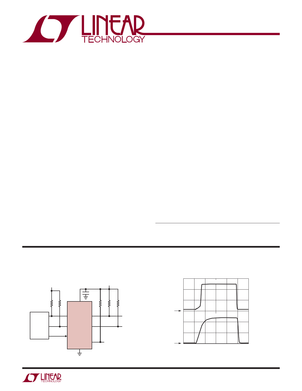
TYPICAL APPLICATION
The LTC4308 in a 1.2V
Microcontroller Application
1.2V 5V
0.01μF
MICRO-
CONTROLLER
2.7k 2.7k
VCC
LTC4308
SCLIN SCLOUT
SDAIN SDAOUT
ENABLE
READY
GND
10k 2.7k 2.7k
READY
CARD_SCL
CARD_SDA
4308 TA01a
2V/DIV
CH1
1.2V to 5V Level Shifting
SDAOUT
0.5V/DIV
CH2
SDAIN
1μs/DIV
4308 TA01b
4308f
1
1 page 
LTC4308
TYPICAL PERFORMANCE CHARACTERISTICS TA = 25°C, VCC = 3.3V, unless otherwise indicated.
ICC Enabled Current
vs Temperature
8.0
ISD Disabled Current
vs Temperature
1000
7.5
VCC = 5.5V
7.0
6.5
VCC = 3.3V
6.0
VCC = 2.3V
5.5
950
900
850
800
750
5.0 700
4.5 650
4.0
–50 –25
0
25 50
TEMPERATURE (°C)
Input-Output High to Low
Propagation Delay
vs Temperature
140 CIN = COUT = 50pF
RPULLUPIN = RPULLUPOUT = 2.7k
120
75 100
4308 G01
600
–50 –25
0
25 50
TEMPERATURE (°C)
75 100
4308 G02
Boost Pull-Up Current
vs Temperature
24
CIN = 50pF, COUT = 1nF
RPULLUPIN = RPULLUPOUT = 2.7k
20
100
VCC = 5.5V
80
VCC = 2.3V
60
VCC = 3.3V
16 VCC = 5.5V
12
8 VCC = 3.3V
4 VCC = 2.3V
40
–50 –25
0
25 50 75 100
TEMPERATURE (°C)
0
–50 –25
Input-Output High to Low
Propagation Delay vs Output
Capacitance
140 CIN = 50pF
RPULLUPIN = 2.7k
125 RPULLUPOUT = 2.7k
4308 G03
Input-Output Offset Voltage
vs Pull-Up Resistance
–196
–198
0 25 50
TEMPERATURE (°C)
75 100
4308 G04
Output-Input Offset Voltage
vs Pull-Up Resistance
304
302
110
95
80
65
50
0
VCC = 5.5V
VCC = 2.3V
VCC = 3.3V
VPULLUPIN = 1.8V
VPULLUPOUT = VCC
200 400 600 800 1000
OUTPUT CAPACITANCE (pF)
4308 G05
–200
–202
–204
–206
0
2 4 6 8 10
INPUT BUS PULL-UP RESISTANCE (k)
4308 G06
300
298
296
294
0 2 4 6 8 10
OUTPUT BUS PULL-UP RESISTANCE (k)
4308 G07
4308f
5
5 Page 
LTC4308
APPLICATIONS INFORMATION
Resistor Pull-Up Value Selection
To guarantee the SDAOUT and SCLOUT rise time accelera-
tors are activated during a rising edge, the bus must rise
on its own with a positive slew rate of at least 0.8V/μs. To
achieve this, choose a maximum resistor value RPULLUP
using the formula:
RPULLUP
≤
(VBUS(MIN)
−
0.8V)•
CBUS
1250ns
/
V
Where RPULLUP is the pull-up resistor value in kΩ, VBUS(MIN)
is the minimum bus pull-up supply voltage and CBUS is
the equivalent bus capacitance in pF.
To estimate the value of CBUS, use a general rule of 20pF
of capacitance per device on the bus (10pF for the device
and 10pF for interconnect).
In addition, RPULLUP must be strong enough to overcome
the precharge voltage and provide logic highs on SDAOUT
and SCLOUT for the start-up and connection circuitry to
connect the backplane to the card. To meet this require-
ment, always choose
RPULLUP
≤
75k
VBUS(MIN) − VTHR(MAX)
VTHR(MAX) − 1V
where VTHR(MAX) is the maximum specified Logic Input
Threshold Voltage, VTHR.
Further, on SDAIN and SCLIN and for heavily loaded
systems on SDAOUT and SCLOUT, where the selected
RPULLUP value causes the bus to rise at a rate slower than
0.8V/μs, users must also guarantee
RPULLUP
≤
VBUS(MIN) − VTHR(MAX)
100μA
Live Insertion and Capacitance Buffering Application
Figure 4 and 5 illustrate applications of the LTC4308 that
take advantage of the LTC4308’s Hot Swap™, capacitance
buffering and output pin precharge features. If the I/O
cards were plugged directly into the backplane without the
LTC4308 buffer, all of the backplane and card capacitances
would add directly together, making rise time and fall time
requirements difficult to meet. Placing an LTC4308 on the
edge of each card isolates the card capacitance from the
backplane. For a given I/O card, the LTC4308 drives the
capacitance of everything on the card and the backplane
must drive only the capacitance of the LTC4308, which
is less than 10pF.
Figure 4 shows the LTC4308 used in the typical staggered
connector application, where VCC and GND are the longest
“early power” pins. The “early power” pins ensure the
LTC4308 is initially powered and forcing the 1V precharge
voltage on the medium length SDA and SCL output pins
before they contact with the backplane busses. Coupled
with ENABLE as the shortest pin, passively pulled to ground
by a resistor, the staggered approach provides additional
time for transients associated with live insertion to settle
before the LTC4308 can be enabled.
Figure 5 shows the LTC4308 in an application where all
of the pins have the same length. In this application, a
resistor is used to hold the ENABLE pin low during live
insertion, until the backplane control circuitry can enable
the device.
Level Shifting Applications
Systems requiring different supply voltages for the
backplane side and the card side can use the LTC4308
for bidirectional level shifting, as shown in Figures 4, 5,
and 7. The LTC4308 can level shift between bus pull-up
supplies as low as 0.9V to as high as 5.5V. Level shifting
allows newer designs that require lower voltage supplies,
such as EEPROMs and microcontrollers, the capability to
interface with legacy backplanes which may be operating
at higher supply voltages.
The LTC4308’s negative offset voltage from output to
input allow level shifting applications with high SDAOUT
and SCLOUT VOL to effectively translate to the low voltage
SDAIN and SCLIN busses. Figure 7 shows an application
where 200Ω resistors, used to provide additional ESD
protection for the Temperature Sensor’s internal low
impedance pull-down device, generate high VOL on the
SDAOUT and SCLOUT busses.
4308f
11
11 Page | ||
| Páginas | Total 16 Páginas | |
| PDF Descargar | [ Datasheet LTC4308.PDF ] | |
Hoja de datos destacado
| Número de pieza | Descripción | Fabricantes |
| LTC4300-1 | (LTC4300-1/-2) Hot Swappable 2-Wire Bus Buffers | Linear Technology |
| LTC4300-2 | (LTC4300-1/-2) Hot Swappable 2-Wire Bus Buffers | Linear Technology |
| LTC4300A-1 | (LTC4300A-1/-2) Hot Swappable 2-Wire Bus Buffers | Linear Technology |
| LTC4300A-2 | (LTC4300A-1/-2) Hot Swappable 2-Wire Bus Buffers | Linear Technology |
| Número de pieza | Descripción | Fabricantes |
| SLA6805M | High Voltage 3 phase Motor Driver IC. |
Sanken |
| SDC1742 | 12- and 14-Bit Hybrid Synchro / Resolver-to-Digital Converters. |
Analog Devices |
|
DataSheet.es es una pagina web que funciona como un repositorio de manuales o hoja de datos de muchos de los productos más populares, |
| DataSheet.es | 2020 | Privacy Policy | Contacto | Buscar |